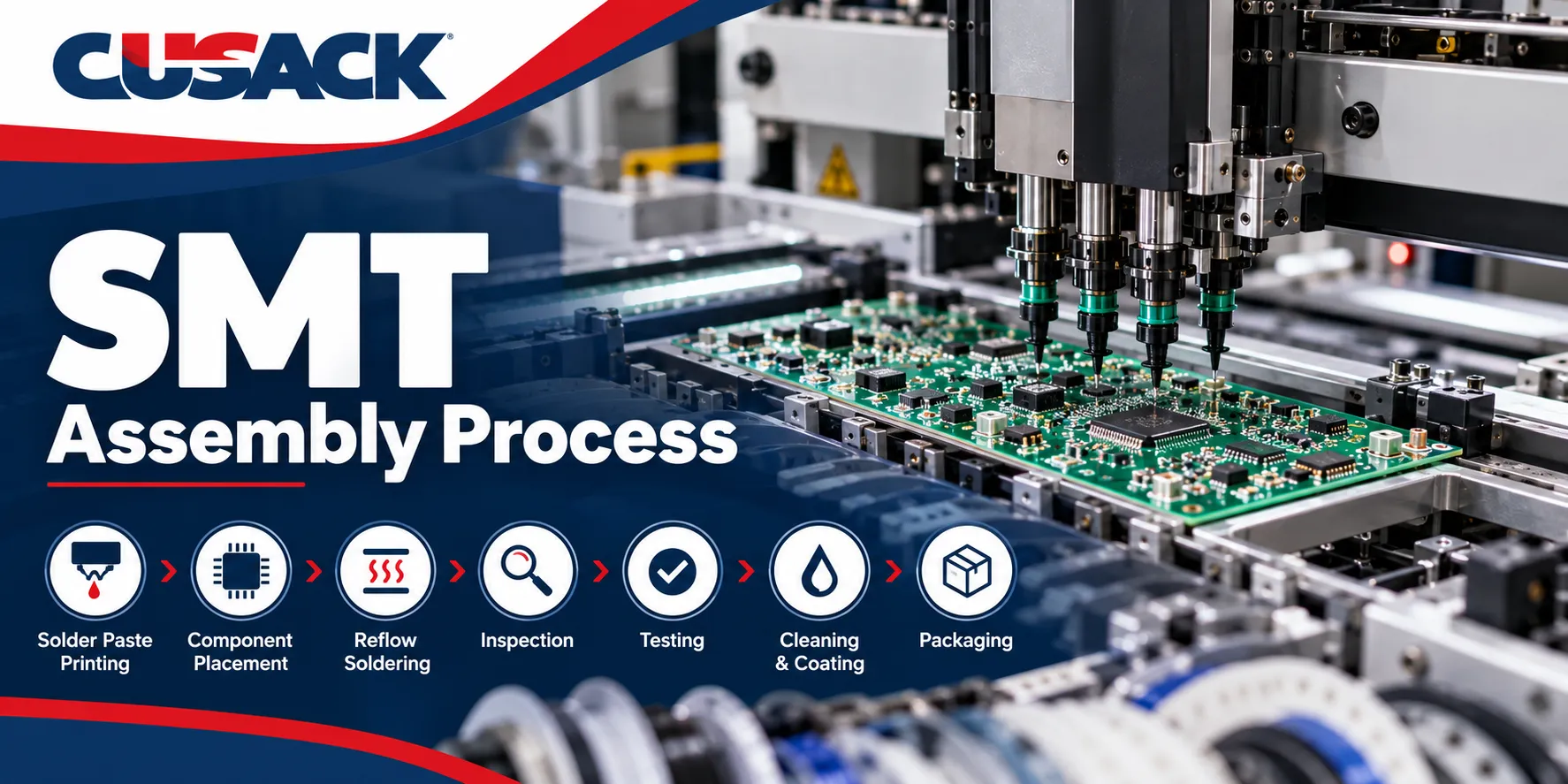
TL;DR: The SMT assembly process turns a bare printed circuit board into a working assembly by soldering surface-mount devices onto pads on the board surface. It runs in seven stages: solder paste printing through a stencil, solder paste inspection, component placement by a pick-and-place machine, reflow soldering, automated optical inspection, electrical test, then cleaning and coating. Paste printing sits first and causes most of the defects, which is why stencil design and paste inspection earn their place on the line.
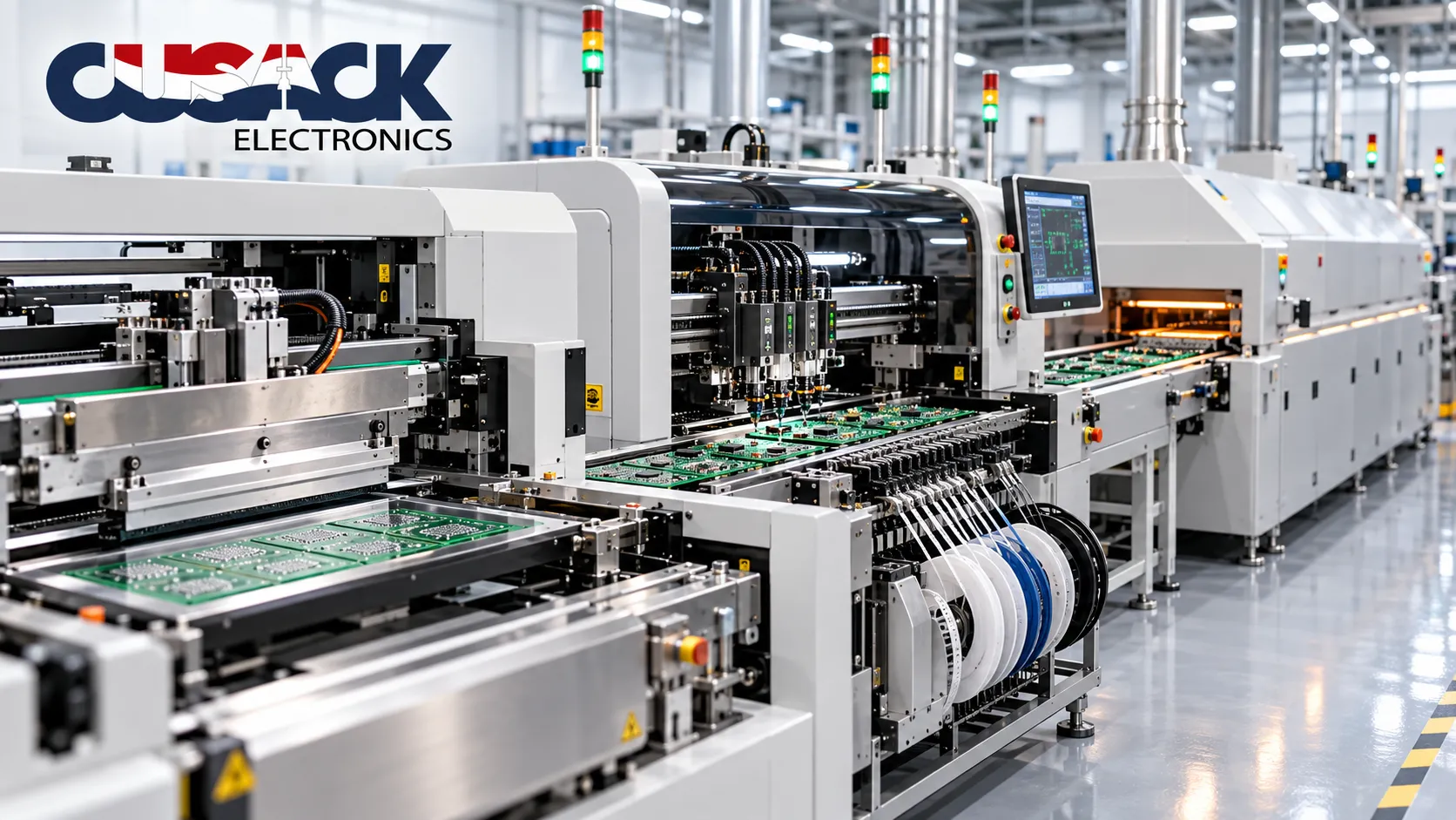
Most explanations of how SMT assembly works hand you seven boxes with arrows between them. The list is accurate. It is also close to useless, because it never says which box decides whether your board works.
I will be straight with you: it is the first one. Solder paste printing produces most of the defects the rest of the line then spends its time catching, and the inspection you pay for downstream is largely cleanup after a bad print.
So every stage below comes with the numbers that matter at it, the standard that governs it, and the failure it tends to produce when it drifts.
What Is the SMT Assembly Process?
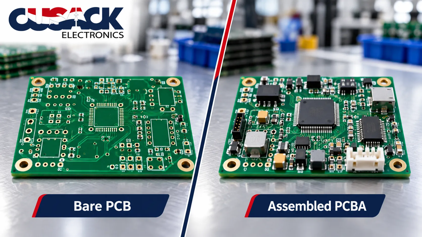
The SMT assembly process is the manufacturing sequence that mounts surface-mount devices (SMDs, components with flat leads or pads instead of wire legs) onto the surface of a printed circuit board and solders them in place using paste and heat.
Think of it like screen printing a T-shirt, then baking it. A stencil lays down a precise pattern of solder paste, a machine sets components into that wet paste, and an oven melts the paste so it pulls tight into finished solder joints as it cools.
Surface-mount technology (SMT) replaced the older method of pushing component legs through drilled holes because it removes the drilling, works on both sides of the board, and handles parts too small to have legs at all.
You will also see this called the SMT manufacturing process, or the SMT PCB assembly process. Same sequence, different labels.
One point of vocabulary first. The bare board is the PCB; the assembled board with components on it is the PCBA. If that distinction is fuzzy, my guide to PCB vs PCBA covers it properly.
The Sequence in Short
Here is the SMT process step by step, as it runs on my floor. Nothing exotic, just the surface mount assembly process in the order the board meets it:
- Solder paste printing: a stencil deposits paste onto every pad.
- Solder paste inspection (SPI): a scanner measures the volume and position of each deposit.
- Component placement: a pick-and-place machine sets each part into the paste.
- Reflow soldering: the board passes through a reflow oven that melts and solidifies the paste.
- Automated optical inspection (AOI): cameras compare every joint against a known-good reference.
- Electrical test: the board is powered and probed to confirm it works.
- Cleaning, coating, and packaging: flux residue comes off, protection goes on.
Everything before step one is preparation, and preparation is where most of the outcome is already decided. For how this sequence sits inside the wider job, including the through-hole and box build stages around it, see my complete guide to PCB assembly.
Before the Line Runs: Data, Stencil, and Materials
Nothing gets switched on until three things are settled: the data package is complete, the stencil is cut, and the parts are on the shelf in a condition fit to solder.
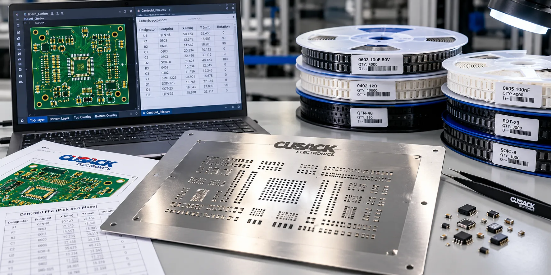
What You Actually Need to Send Me
Four files decide whether a job runs clean or stalls on the first board.
- Gerber files: the layer-by-layer artwork for the board itself.
- The paste layer: the map of every aperture the stencil needs cut. Without it, the stencil gets guessed from the pad layer, and guesses cost yield.
- Centroid (XY) file: the coordinate, rotation, and side for every part, which is what the placement machine reads.
- Bill of materials: manufacturer part numbers, not descriptions. “0.1uF cap” is not a part number.
Rotation errors in the centroid file are the single most common data problem I see. A diode listed at zero degrees that should be at 180 will place perfectly, solder perfectly, and fail test on every board in the batch.
If the design has not been reviewed for manufacturability yet, that review belongs here, before the stencil is cut. I have written separately on design for manufacturability and what it catches.
Whether I buy the parts or you ship them to me changes the schedule more than anything else on this list, which is the subject of turnkey versus consignment assembly.
How the Stencil Gets Designed
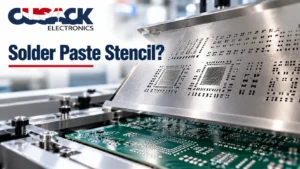
The stencil is a thin stainless steel foil with an aperture cut over every pad. Its thickness and its aperture shapes set how much paste lands on each pad, and paste volume is the variable that most of the downstream defects trace back to.
The governing document is IPC-7525C, *Stencil Design Guidelines*, published in 2021, which replaced IPC-7525B from 2011.
Two ratios do the work. IPC-7525B defines area ratio as the ratio of the area of the aperture opening to the area of the aperture walls, and aspect ratio as the ratio of the width of the aperture to the thickness of the stencil foil.
Here is why that matters in plain terms. Paste has to choose between sticking to the pad and sticking to the inside walls of the aperture as the stencil lifts away.
A wide, shallow aperture gives the paste more pad to grip than wall, so it releases cleanly. A narrow, deep one does the opposite and leaves paste behind in the hole. Most stencil designers work to an area ratio above 0.66 for that reason.
This is also why a board carrying both an 0201 chip resistor and a large connector can need a stepped stencil, thinner over the fine-pitch parts and thicker where bulk paste is wanted.
Moisture-Sensitive Parts and the Bake Question
Plastic-bodied components absorb moisture from the air. Heat that moisture fast enough in a reflow oven, and it turns to steam inside the package, which cracks it. The industry name for that failure is popcorning, and it is as audible as it sounds.
The classification standard is IPC/JEDEC J-STD-020F, *Moisture/Reflow Sensitivity Classification for Non-hermetic Surface Mount Devices*, issued in 2022 to replace J-STD-020E from 2015.
It assigns each package a moisture sensitivity level, which sets how long that part may sit exposed to room air before it must be baked dry or reflowed.
Practically: parts arrive in sealed bags with desiccant and a humidity indicator card. Once a bag is opened, a clock starts. Ignore that clock on a moisture-sensitive BGA, and the cracking happens inside the package where no inspection step will ever see it.
Step 1: Solder Paste Printing
Solder paste printing presses solder paste through the stencil apertures onto the board pads, depositing the exact volume of paste each joint needs.
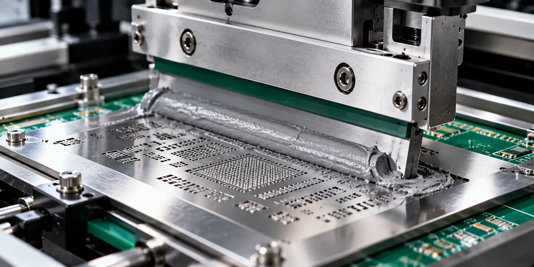
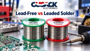
The paste itself is a suspension of tiny solder spheres in flux. The common lead-free alloy is SAC305, roughly 96.5% tin, 3% silver, and 0.5% copper, which becomes fully liquid near 217 degrees Celsius.
The printer clamps the board, aligns the stencil to fiducial marks etched on the board surface, then drags a squeegee blade across at a controlled speed and pressure. The stencil separates, and the paste stays behind on the pads.
Four variables get tuned here: print speed, squeegee pressure, separation speed, and the cleaning interval for the stencil underside. Change any of them and the deposit volume moves.
Paste is also perishable. It comes out of refrigeration, needs time to reach room temperature before the jar is opened, and has a working life on the stencil measured in hours rather than days.
Step 2: Solder Paste Inspection
Solder paste inspection (SPI) scans the printed board in 3D and measures the height, area, volume, and position of every paste deposit before any component is placed.
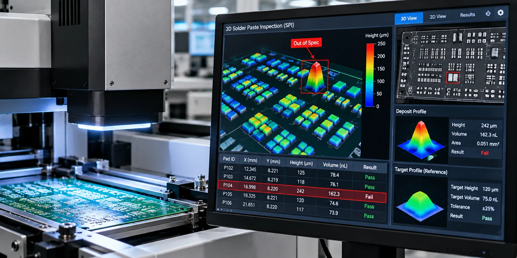
Not every shop runs SPI, and for a simple board with generous pad geometry you can get away without it. I would not skip it on anything carrying fine-pitch parts or bottom-terminated packages.
The reason is economics. A board caught at SPI is wiped clean and reprinted in under a minute. The same fault caught after reflow means rework on a populated board, and caught after test it means a diagnosis first.
SPI is the only station on the line that inspects a cause rather than an effect. Everything after reflow is looking at symptoms.
Step 3: Component Placement
Component placement is the stage where a pick-and-place machine lifts each surface-mount device from a reel, tray, or tube and sets it onto its paste deposit at the coordinates given in the centroid file.
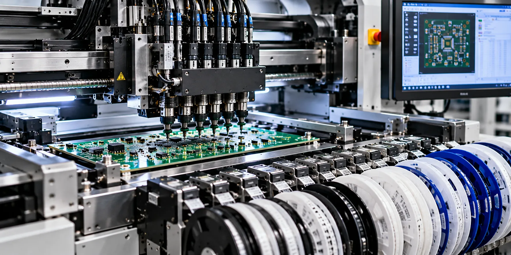
A modern machine works through a rotating head carrying several vacuum nozzles. It picks a part, photographs it in flight to check the part is what it claims to be and is held square, corrects the angle, and places it.
Placement accuracy on current equipment sits in the tens of microns, and a chip-shooter head can pick and place tens of thousands of components per hour.
Nothing is soldered yet. The parts are held only by the tackiness of the wet flux in the paste, which is why boards move gently between this station and the oven.
Feeder setup is where placement time is genuinely lost. Every part the machine will pick and place has to be loaded into a feeder, verified, and mapped to a slot.
A 40-part board and a 400-part board take similar machine time once running. Setting up the 400-part board takes far longer, which is the real reason small batches cost more per unit.
That cost structure is covered in my breakdown of PCB assembly cost.
Step 4: Reflow Soldering
Reflow soldering carries the populated board through a reflow oven on a conveyor, heating it through a controlled temperature curve that melts the solder paste and forms every solder joint at once.
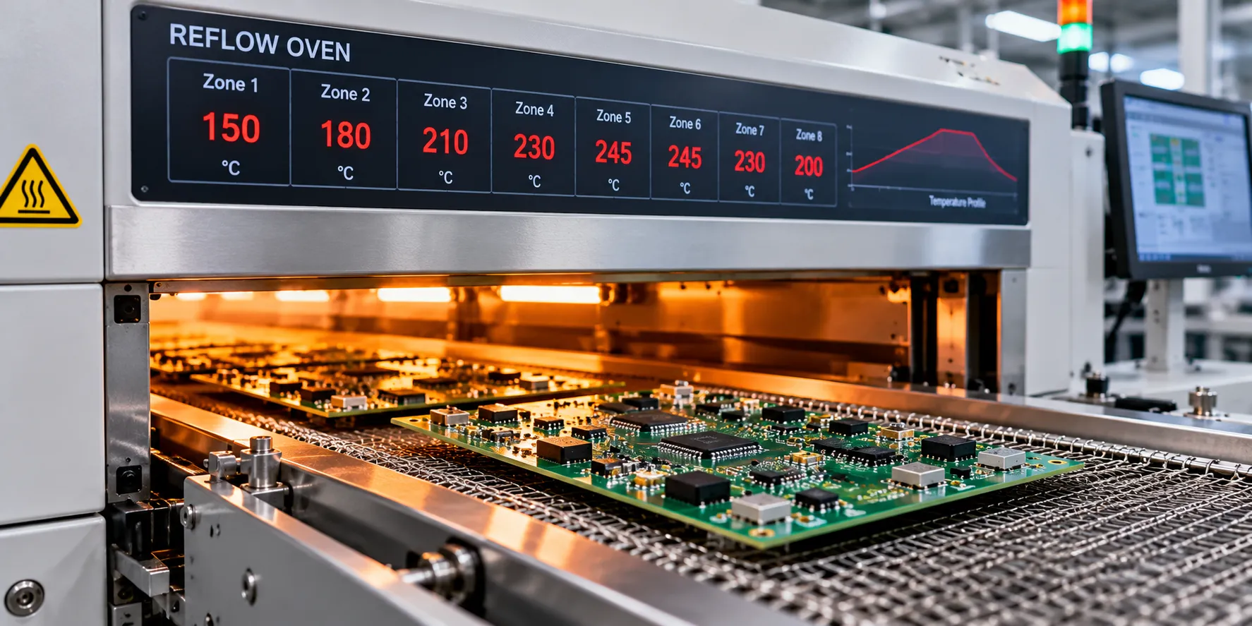
This is the step people picture when they think about the soldering process, and it is the one with the least room for improvisation. A production oven has eight to twelve independently controlled zones, and the board’s own temperature through those zones is what matters, not the zone set points.
The Four Zones of a Reflow Profile
Every reflow profile does the same four jobs in the same order.
- Preheat: raise the board steadily from room temperature. Too fast and thermal shock cracks components; too slow and the flux is spent before it is needed.
- Soak: hold in a band below melting to let the flux clean the oxide off pads and leads, and to let the thin parts and thick parts of the board reach a similar temperature.
- Reflow: cross the alloy’s melting point so the solder liquefies, wets the pad, and pulls the component into alignment through surface tension.
- Cooling: drop the temperature at a controlled rate to set a fine grain structure in the joint.
The time the joint spends above the melting point is called time above liquidus, and it is the number most profiling arguments are about. Too short and the solder never wets properly; too long and you grow brittle intermetallic layers and cook the components.
Why the Peak Temperature Is Not a Free Choice
The peak has to clear the alloy’s melting point with enough margin to wet reliably, and stay under what the least tolerant component on the board can survive.
That upper limit is not a guess. It comes from the classification reflow profile in J-STD-020F for the packages on the board, cross-checked against the paste manufacturer’s own datasheet.
Profile to the paste datasheet and the component ratings, verified with a thermocouple-instrumented board run through the oven. Never profile from a number found in an article, including this one.
Step 5: Automated Optical Inspection and X-Ray
Automated optical inspection (AOI) photographs the soldered board and compares every component and joint against a reference image, flagging anything outside tolerance.
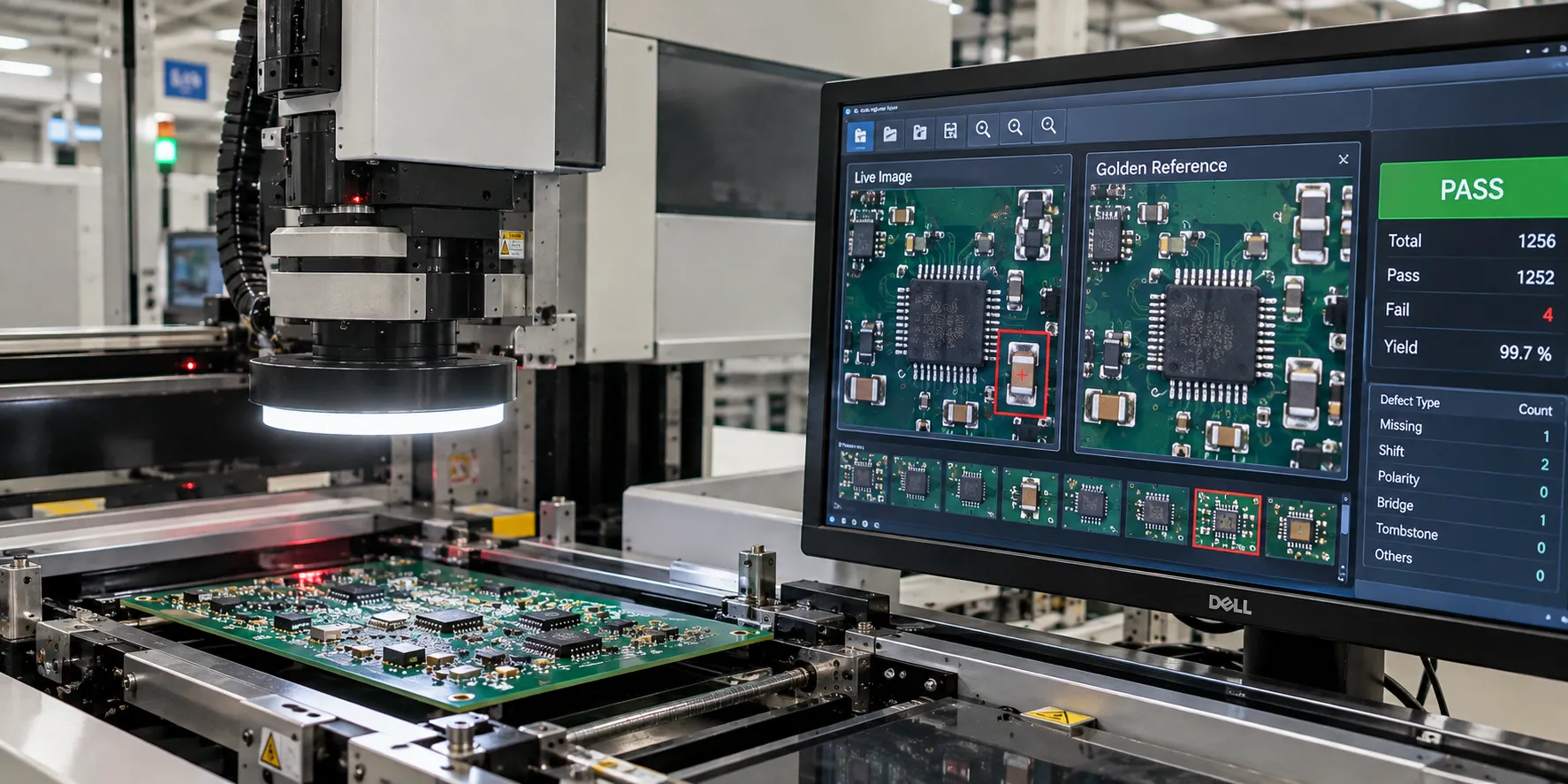
AOI catches the visible faults well: a missing part, a part rotated or offset, a tombstoned resistor standing on one end, a solder bridge between two pins, insufficient solder on a visible fillet.
The acceptance criteria it is judged against come from IPC-A-610, the standard that defines what an acceptable solder joint looks like at each of the three IPC classes.
What AOI cannot do is see underneath a part. A ball grid array (BGA) or a quad-flat no-lead (QFN) package hides its joints beneath the body, and a camera has no angle on them.
That is what X-ray inspection is for. It looks through the package to find voids, bridges, and open joints on connections no optical system can reach, which is why boards with BGAs get X-rayed and simple boards usually do not.
Step 6: Electrical Test
Electrical test powers the assembled board and confirms it behaves the way the design says it should, which is the first point in the process where anyone learns whether the thing actually works.
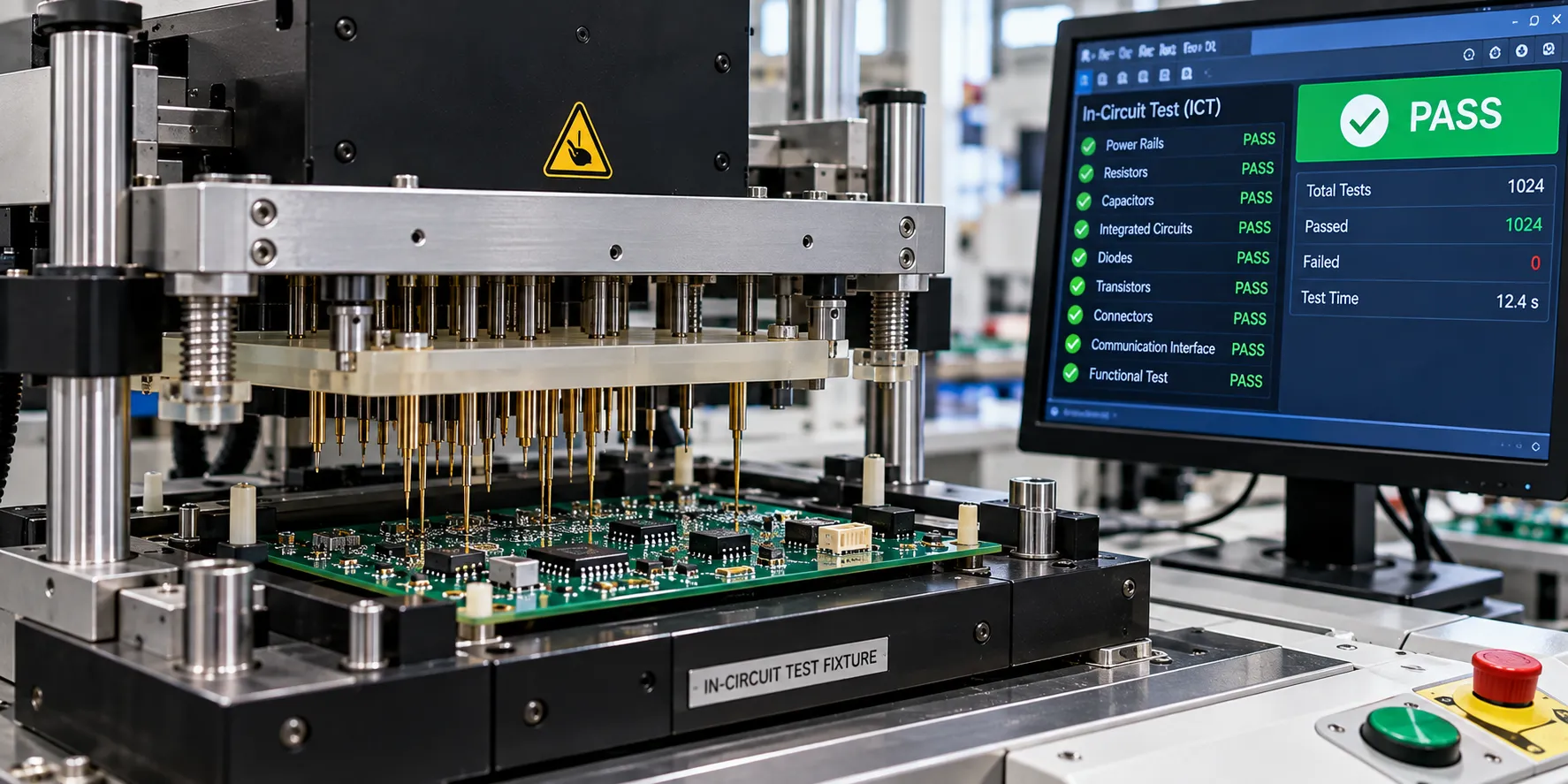
Two approaches cover most work. In-circuit test (ICT) uses a fixture of spring probes to contact test points and measure individual components in place, while functional test (FCT) runs the board as the finished product and checks its outputs.
ICT finds the manufacturing fault and tells you which part is wrong. Functional test finds the symptom the customer would have found. Useful boards get both where volume justifies the fixtures.
Flying probe test is the middle path for low volumes: slower per board, but no fixture to build, which makes it the sensible choice for prototypes and short runs.
I have gone through the full set of options in my guide to PCB testing methods.
Step 7: Cleaning, Coating, and Packaging
The final stage removes flux residue where the assembly requires it, applies any protective coating, and packages the boards for shipment or for the next assembly stage.
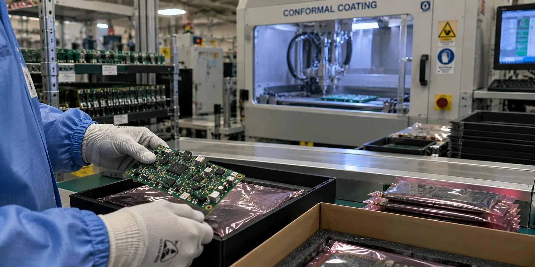
Most work now uses no-clean flux, where the residue is formulated to stay put harmlessly. Cleaning still happens for medical, aerospace, and any board getting a conformal coating, because coating over active residue traps a problem underneath it.
Coating protects against moisture, dust, and chemical exposure. The choice between acrylic, silicone, urethane, and parylene depends on the environment, and I have compared them in detail in my piece on conformal coating.
On a first production run, this is also where first article inspection lands: one board fully checked and signed off before the rest of the batch continues. That sits inside the wider new product introduction process.
Double-Sided and Mixed-Technology Boards
A board with components on both sides runs the whole SMT sequence twice, bottom side first, then top.
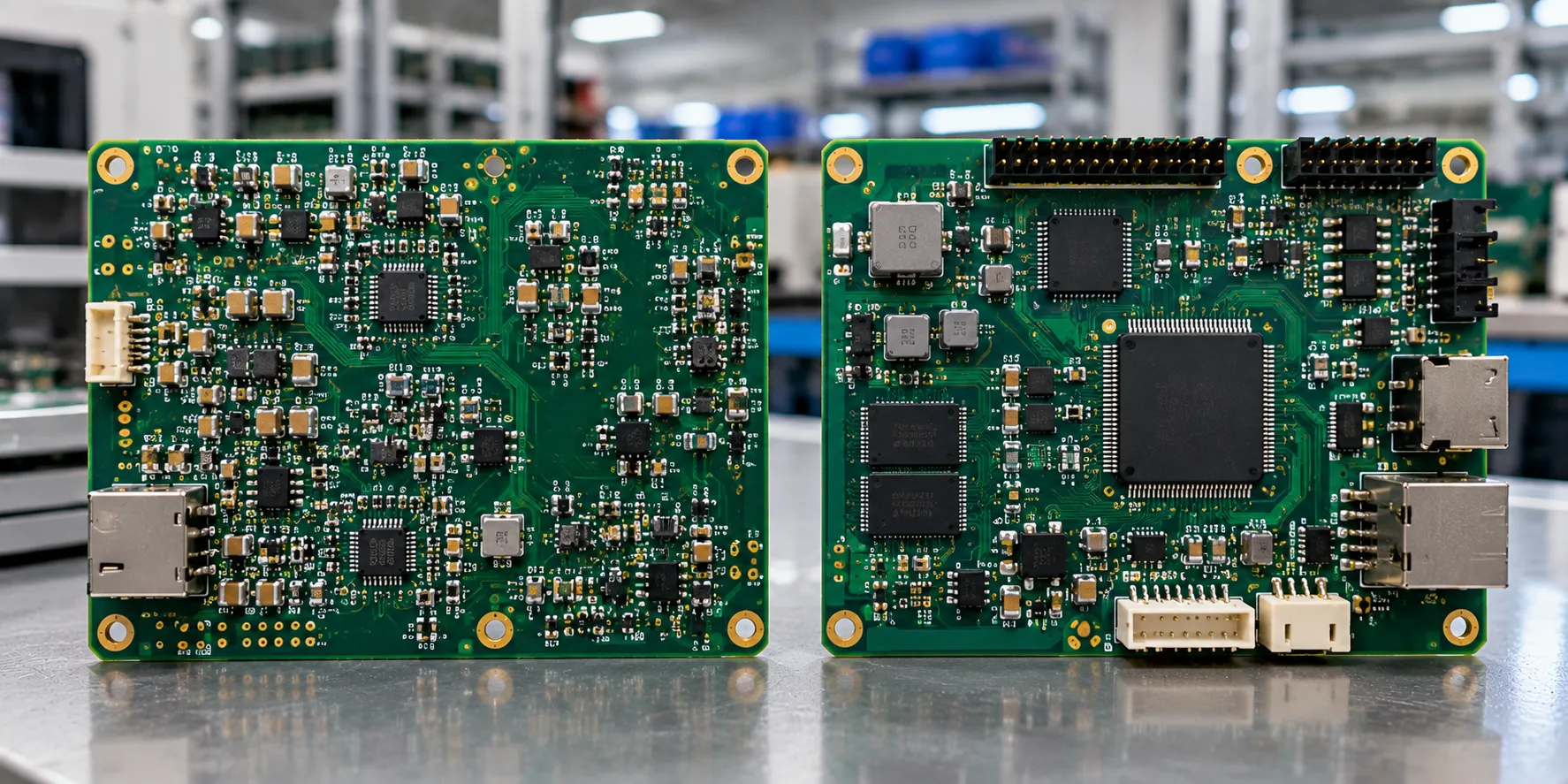
The bottom side gets the smaller, lighter parts and goes through reflow first. On the second pass the board is inverted, and surface tension in the molten solder holds those first-side parts in place as long as they are light enough. Heavy parts on the bottom get glued or moved to the top instead.
Then there are the parts that have no surface-mount version worth using: power connectors, transformers, anything that takes mechanical abuse. Those are through-hole, and they are fitted after SMT reflow, by selective soldering or by hand.
Almost every real board is a mix of both technologies. I have compared them directly, including where each one fails, in SMT vs through-hole.
Defects, and the Step That Caused Them
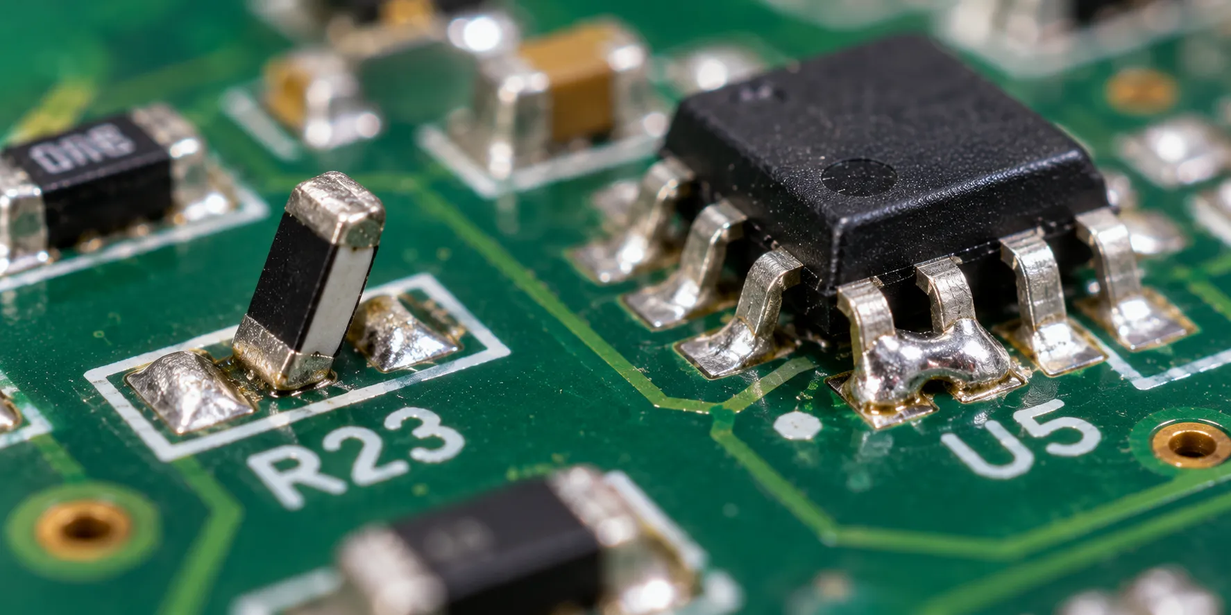
Most SMT defects are traceable to a specific station. Knowing which one turns a scrap board into a process correction.
| Defect | What it looks like | Usual origin |
|---|---|---|
| Tombstoning | A two-lead chip part standing upright on one end | Uneven paste volume or uneven heating across the two pads |
| Solder bridging | Solder joining two pads that should be separate | Too much paste, smeared print, or misalignment |
| Insufficient solder | A thin, starved fillet | Blocked stencil aperture or poor paste release |
| Head-in-pillow | A BGA ball touching the pad but never merging with it | Board or component warping during reflow, or spent flux |
| Voiding | Gas pockets trapped inside a joint, visible only on X-ray | Paste chemistry, profile, and pad or via design |
| Cold joint | A dull, grainy joint that never fully melted | Peak temperature or time above liquidus too low |
| Component cracking | Fractured package body, often invisible externally | Moisture absorbed before reflow, or preheat ramp too steep |
Look at the origin column. Four of the seven start at the printer, which is the case for putting a paste inspection step on the line.
How Long Does the SMT Assembly Process Take?
Machine time per board is short. Setup time is not, and that gap explains most of what people find surprising about assembly lead times.
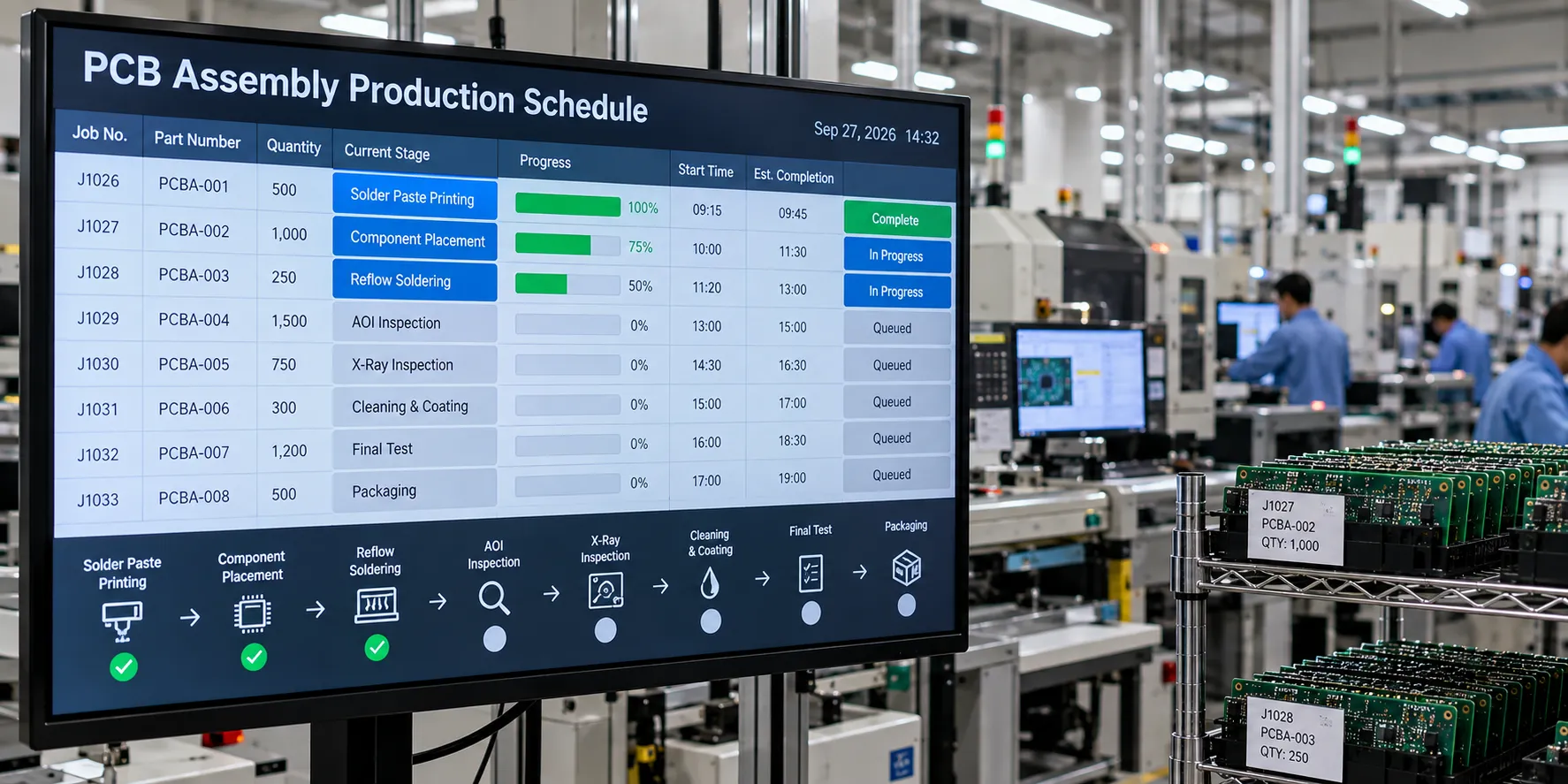
Once a line is set up and running, a modest board clears the whole sequence in minutes. The reflow oven alone accounts for four to six of them, since the conveyor speed has to match the profile.
The work that takes real time sits before that: reviewing the data package, cutting the stencil, waiting on component lead times, loading and verifying feeders, then running and approving a first article.
Component availability is usually the long pole. A board can be ready to run for weeks while one part is on back order, which is the single most common reason a schedule slips.
Frequently Asked Questions
What are the steps of the SMT assembly process?
Solder paste printing, solder paste inspection, component placement by pick-and-place machine, reflow soldering, automated optical inspection, electrical test, then cleaning, coating, and packaging. Double-sided boards repeat the first four steps for the second side.
What is the difference between SMT and SMD?
SMT is the process, SMD is the part. Surface-mount technology is the method of assembly; a surface-mount device is an individual component built to be assembled that way.
Do I need solder paste inspection on every board?
No. On simple boards with generous pad spacing, AOI after reflow catches enough. On fine-pitch or bottom-terminated parts, SPI pays for itself quickly, because reprinting a board costs a minute and reworking one costs far more.
What temperature does SMT reflow run at?
It depends on the alloy and the components. Lead-free SAC305 becomes liquid near 217 degrees Celsius and peaks above that, but the correct profile for any given board comes from the solder paste datasheet and the component moisture and temperature ratings, verified with a thermocouple-instrumented test board.
Can through-hole components go through an SMT line?
Not through reflow in the normal way. Through-hole parts are fitted after SMT reflow using selective soldering, wave soldering, or hand soldering. Press-fit connectors avoid soldering entirely.
Why did my boards fail after assembly when the components are correct?
Check component rotation in the centroid file first. A polarised part placed at the wrong angle solders perfectly and fails every board in the batch identically, which is the pattern that points at data rather than process.