What You Learn in 30 Seconds
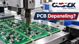
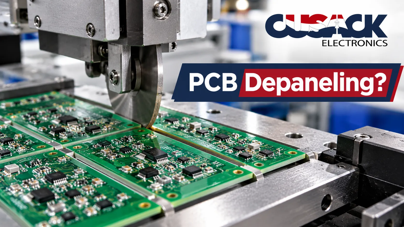
PCB depaneling is the step that separates individual boards from the production panel they were built on. The usual methods are V-scoring, tab routing, sawing, punching, routing and UV laser cutting, and they differ mainly in how much mechanical stress they put into the board. That stress is the part most guides skip. Three ceramic capacitor manufacturers independently name depaneling as a leading cause of hidden cracks, one of them measured it as the highest-strain process in the whole assembly sequence, and none of them will tell you how far to keep parts away from the break line.
PCB depaneling gets treated as the boring last step. Snap the boards apart, box them up, done.
I would argue it is the most under-respected operation on the line. It is the only point where you deliberately apply force to a finished assembly, and the damage it causes is invisible to the tests most people run afterwards.
So here is my flat opinion before the detail: if you have unexplained field failures and a hand-break process, look at depaneling before you look at anything else.
What Is PCB Depaneling?
PCB depaneling is the process of separating individual circuit boards from the larger panel they were manufactured and assembled on.
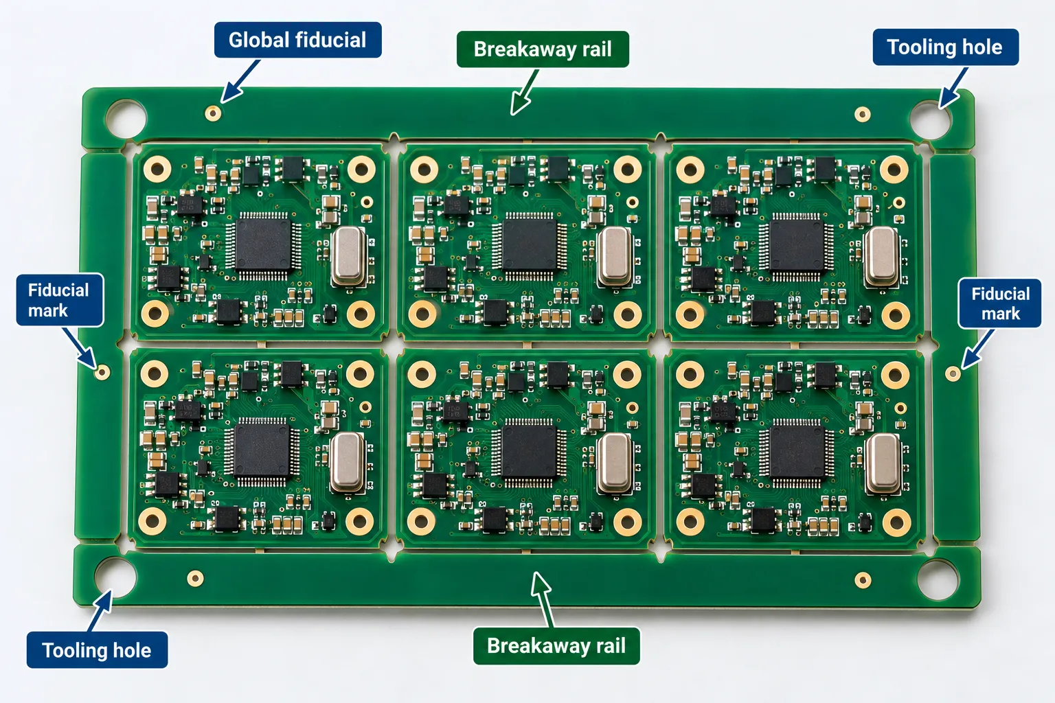
Boards are built in panels because the machines demand it. A pick-and-place machine, a stencil printer and a reflow oven all want a consistent, handleable rectangle, and a panel of six small boards runs in roughly the time one would.
Think of it like a sheet of stamps. The whole sheet goes through the press as one piece, and the perforations exist so you can take one stamp off later without tearing the rest.
PCB panelization is the design side of that: deciding how many boards fit, how they are held together and where the separation lines go. Depaneling, also called singulation, is the manufacturing step that undoes it.
The panel design has to be decided before the first board is fabricated, which makes it a design for manufacturability question rather than a production one.
Separation sits near the end of the PCB assembly sequence but gets decided at the very start of it.
What Are the Main PCB Depaneling Methods?
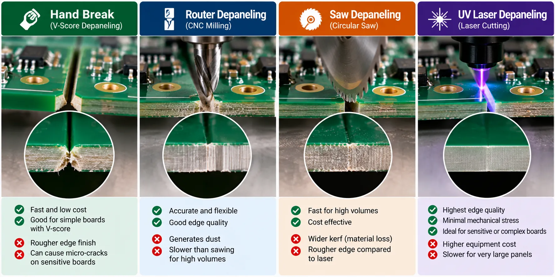
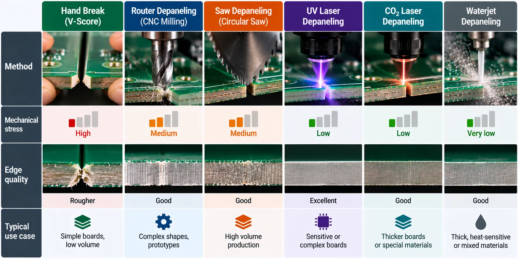
There are six PCB depaneling methods in common use, and the honest way to compare them is by stress and edge quality rather than by speed.
| Method | How it separates | Stress | Best for |
|---|---|---|---|
| Hand break | Operator snaps along a V-groove | Highest | Simple boards, no parts near the line |
| Pizza cutter | Rotary blade follows the V-groove | Moderate | Straight-line panels, low capital cost |
| Saw | Rotary blade cuts through | Moderate | Straight cuts, scored or unscored, low dust |
| Punch | Hard tooling stamps boards out | Moderate to high | Very high volume, fixed design |
| Router | Milling bit cuts away the tabs | Low | Curved outlines, mixed shapes |
| UV laser | Focused beam ablates material | Lowest | Thin boards, fine pitch, tight clearances |
A depaneling router is the workhorse for anything that is not a plain rectangle, because a milling bit can follow an arc or an internal corner that a blade cannot.
Laser depaneling is the stress-free option and the expensive one. The current technology is a 355 nm UV laser, which ablates material rather than melting it, and the practical ceiling is around 1 mm of board thickness.
Above that the beam has to make repeated passes and the economics stop working, which is why laser sits with thin boards, flex and rigid-flex rather than with standard 1.6 mm FR-4.
V-Scoring vs Tab Routing: Which Should You Use?
The v scoring vs tab routing choice comes down to board shape. Choose V-scoring for rectangular boards packed edge to edge, and tab routing for anything with a shaped outline or a connector that overhangs.
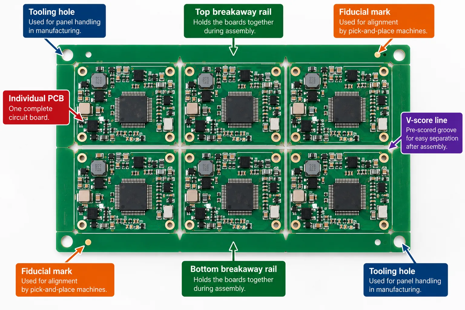
A v score PCB carries a groove cut into the top and bottom faces along each separation line, usually to about a third of the board thickness from each side, leaving a thin web in the middle that breaks cleanly.
The limitation is geometric. A V-score is a straight line that runs the full width of the panel, so every board on that line has to be a rectangle with its edge in the same place.
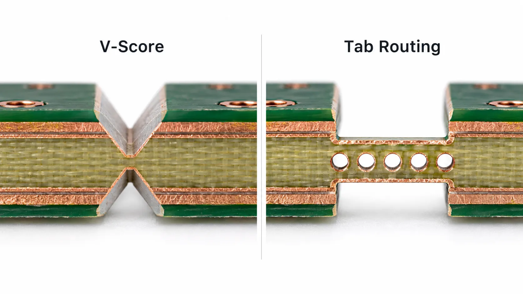
Tab routing cuts the board outline away and leaves small tabs holding each board in place. Those tabs usually carry a row of drilled holes, which is where the name mouse bites comes from, and breaking them leaves the characteristic scalloped edge.
PCB breakaway tabs buy you freedom of shape and cost you edge finish. After a tab route, the stub has to be sanded or accepted, and on a product with a visible edge that matters.
| V-scoring | Tab routing | |
|---|---|---|
| Board outline | Rectangles only | Any shape |
| Edge finish | Clean, straight | Scalloped, may need dressing |
| Panel utilisation | Higher, boards abut | Lower, routing gap between boards |
| Separation stress | Higher, bends the whole line | Lower, localised at tabs |
| Parts near the edge | Poor tolerance | Better, if tabs are placed well |
Mixing both on one panel is normal and usually correct. V-score the straight sides, tab route the shaped end.
Why Does Depaneling Crack Capacitors?
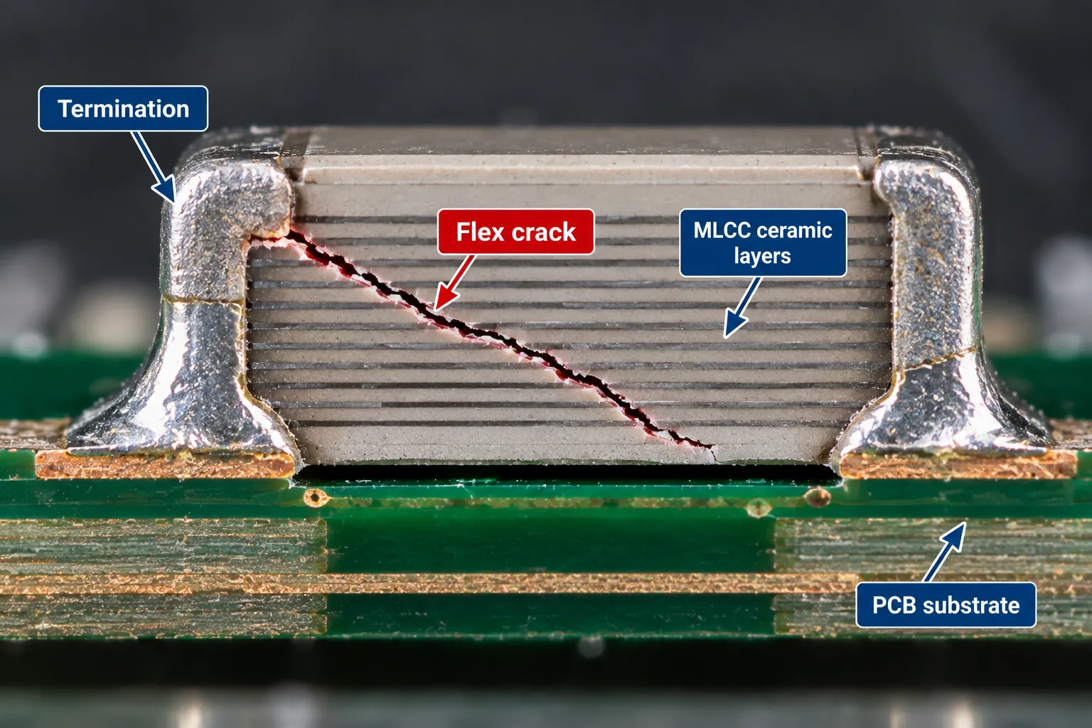
Depaneling bends the board, and multilayer ceramic capacitors crack when the board bends, because ceramic is strong in compression and weak in tension.
This is the part of the subject with real evidence behind it, and none of the depaneling guides I read while researching this mention any of it.
Kyocera measured strain across a full assembly sequence with gauges bonded to the board. It reported that the largest strain occurred in the cropping process, their term for board separation.
Not placement. Not reflow. Separation.
TDK puts numbers on what that strain does. In its 2017 flex crack guidance, a conventional 3216 size capacitor cracked at roughly 4 mm of board flex, soft-termination parts took about twice that, and metal-capped parts survived 10 mm or more.
That document names depaneling as a major cause and tells designers to keep capacitors away from separation areas.
Source: TDK flex crack countermeasures
KYOCERA AVX reaches the same conclusion from the failure-analysis side, calling board depanelization one of the most common areas for fracture failures.
Here is why this matters more than it sounds. A flex crack frequently does not change capacitance or Q, so the part measures fine on a tester. It shows up later, when moisture reaches the crack and creates a low-resistance path.
And the end state is not a dead circuit. KYOCERA AVX notes that a shorted capacitor on a 12 V or 48 V rail carrying a few amps can reach around 1000 degrees Celsius.
Source: KYOCERA AVX on capacitor crack failures
All three of those sources sell capacitors, so it is worth having one from outside the industry. NASA Goddard published a study of stresses in ceramic capacitors that lists de-paneling first among the causes of board deflection cracking, ahead of test probing, screw attachment and connector insertion.
It also describes the crack geometry. They start at the bottom surface near the edge of the termination and run at roughly 45 degrees into the body.
Source: NASA on stresses in ceramic capacitors
One thing that paper does not settle is whether the solder alloy matters. Lead-free solder is stiffer, which ought to transmit more board flex into the ceramic, but it cites data where lead-free assemblies cracked less than tin-lead ones.
I would not design around either direction on that evidence. The wider alloy trade-offs are in my guide to lead-free vs leaded solder.
So the failure mode is an invisible defect, created at the last step, that passes electrical test and can become a fire risk months into service. That is why I treat depaneling as a process to validate rather than a job to hand to whoever is free.
How Far From the Break Line Should Components Sit?
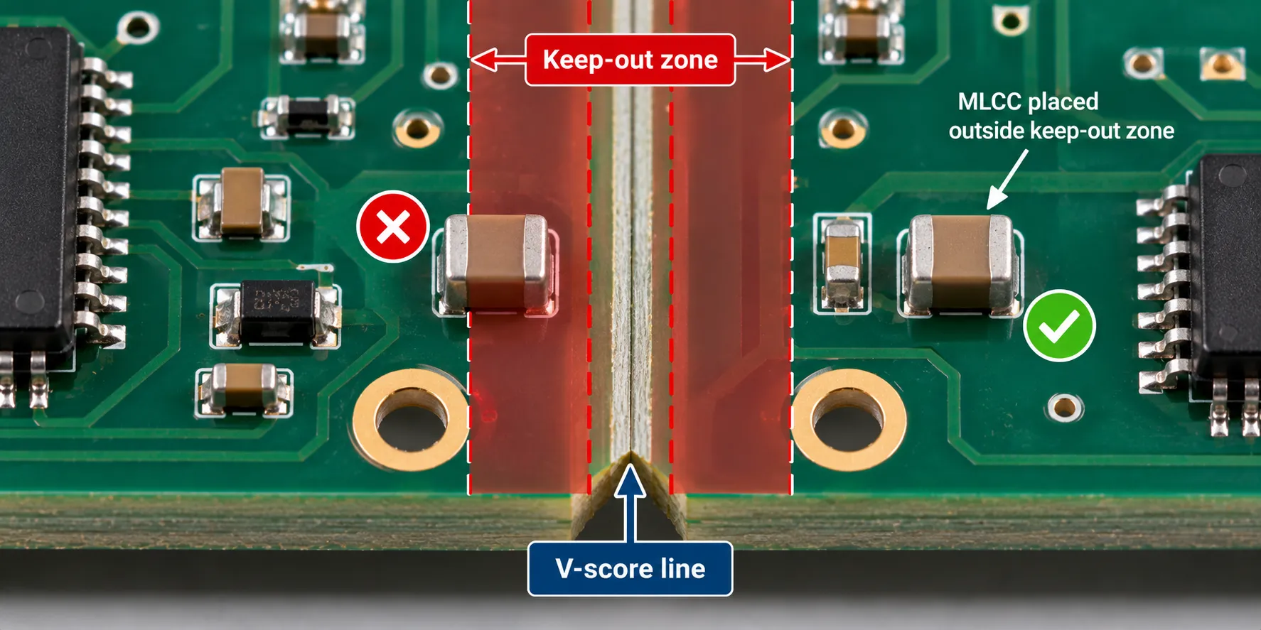
Far enough that the board flex at the part stays below its cracking threshold, which sounds precise and is not, because nobody authoritative publishes the distance.
I went looking for it properly. TDK says keep capacitors away from depaneling areas and gives no distance. KYOCERA AVX says parts too close to the board edge are a common failure point and gives no distance.
The figures in circulation come from fabricators rather than from component makers or a standard. One published panelization guideline sets a minimum of 6.5 mm from the nearest tab, which is a reasonable working number and not one you should treat as a law of physics.
The standard that would settle it is IPC/JEDEC-9704A, the printed circuit assembly strain gauge test guideline. It tells you how to measure board strain properly, which is genuinely useful.
It is still at revision A from 2012, superseding the 2005 original, and its scope covers assembly, test and system integration without naming depaneling specifically.
So the practical approach, in the absence of a number you can cite:
- Keep ceramic capacitors off the break line by the largest margin the layout allows. Several millimetres, more if you can.
- Orient long parts so the break bends them least, and treat large ceramics near an edge as a design review item.
- Prefer soft-termination or metal-cap parts near panel edges when the layout genuinely cannot move them.
- Measure rather than assume. If the product matters, bond a gauge to a sacrificial board and run your actual separation process, following the method in IPC/JEDEC-9704A.
- Choose a lower-stress method before you redesign the board. Moving from hand break to router is usually cheaper than a respin.
That last point is the one I push hardest with customers, because it is reversible and a layout change is not. The component placement decisions are harder to undo once the board is in production.
What Does a Panel Need Besides the Boards?
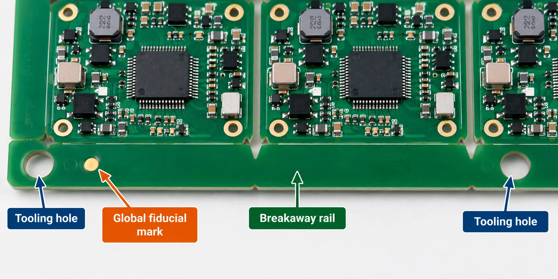
A production panel needs three features that are not part of any board on it, and leaving them out is the most common panelization mistake I see on a first build.
- Panel rails. Strips of bare laminate along two or four edges, typically 5 to 10 mm wide, that give the conveyor and the board clamps something to hold. Without rails the machines grip your circuitry.
- Tooling holes. Precisely located holes used to register the panel in the stencil printer and the placement machine. They sit in the rails, not in the boards.
- Fiducial marks. Small copper targets the vision system uses to find the panel and correct for skew. A panel needs global fiducials on the rails, and fine-pitch parts need local fiducials next to them.
Those three features are what let the panel travel the SMT assembly process at all. They are also why the panel drawing has to exist before the solder paste stencil is cut, since the stencil is made for the panel rather than for one board.
Board-level design rules have a standard behind them, IPC-2221C from 2023. The panel separation geometry mostly does not, because your fabricator’s blade, bit and tolerance capability set it.
They also cost you area. Rails and routing gaps are laminate you pay for and throw away, so panel utilisation feeds straight into PCB assembly cost.
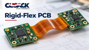
Flex and rigid-flex panels follow different rules again, because the material will not hold itself flat. I have covered that separately in my guide to rigid-flex PCBs.
The Bottom Line
- Depaneling is the separation step. Panelization is the design decision that sets it up, and it has to happen first.
- Six methods in common use. Hand break is the highest stress, UV laser the lowest, router the best general compromise.
- V-score for rectangles packed tight. Tab route for shaped outlines. Mixing both on one panel is normal.
- Depaneling measured as the highest-strain step in a full assembly sequence, per Kyocera.
- Cracked ceramics often pass electrical test and fail later, and a shorted part can reach around 1000 degrees Celsius.
- No component maker or standard publishes a keep-out distance. Fabricator guidance is what exists.
- Changing the separation method is reversible. Moving parts on a finished layout is not.
A cracked capacitor will not show up on a standard functional test, which is worth keeping in mind when you choose your PCB testing methods. If you want a panel design reviewed before the first build, that is a conversation worth having early.
Frequently Asked Questions
What is the difference between panelization and depaneling?
Panelization is the design task of arranging multiple boards on one manufacturing panel and deciding how they are joined. Depaneling, also called singulation, is the physical step of separating them afterwards.
One happens in CAD before fabrication, the other on the production floor after assembly. Getting the first wrong limits your options for the second.
Can you depanel a board by hand?
Physically yes, on a V-scored panel. I would avoid it on anything carrying ceramic capacitors near the break line, because hand breaking produces the highest board flex of any method and the resulting cracks do not show up on a standard test.
A hand fixture that supports the board on both sides of the groove is a cheap improvement over bare hands.
What is a depaneling machine and do I need one?
A depaneling machine is automated equipment that separates panels: usually a router with a milling spindle and a fixture, a saw, or a laser system. You need one when volume, repeatability or stress control justifies it.
For low volumes a pizza cutter or a supported hand fixture is often enough, and the machine becomes worthwhile once scrap from inconsistent separation costs more than the equipment.
How deep is a V-score cut?
Typically about one third of the board thickness from each face, leaving a web in the middle. The precise figure is specified as remaining web thickness rather than depth, and it varies with laminate type and board thickness.
Your fabricator sets this from their blade and tolerance capability, so ask for their figure rather than copying one from a guide.
Does laser depaneling work on every board?
No. UV laser depaneling suits boards up to roughly 1 mm thick, which covers flex, rigid-flex and thin rigid boards well. Standard 1.6 mm FR-4 needs multiple passes and the throughput drops sharply.
It is the right answer when mechanical stress or tight component clearance rules out everything else, and an expensive one otherwise.
Which depaneling method puts the least stress on the board?
UV laser, because nothing touches the board. Routing is next, since the cutting forces stay local to the tab rather than flexing the whole panel.
Hand breaking is the worst by a wide margin. If you cannot change the method, moving to a supported fixture and separating before, not after, any socketed or heavy components go on will reduce the flex considerably.