THE 30-SECOND VERSION
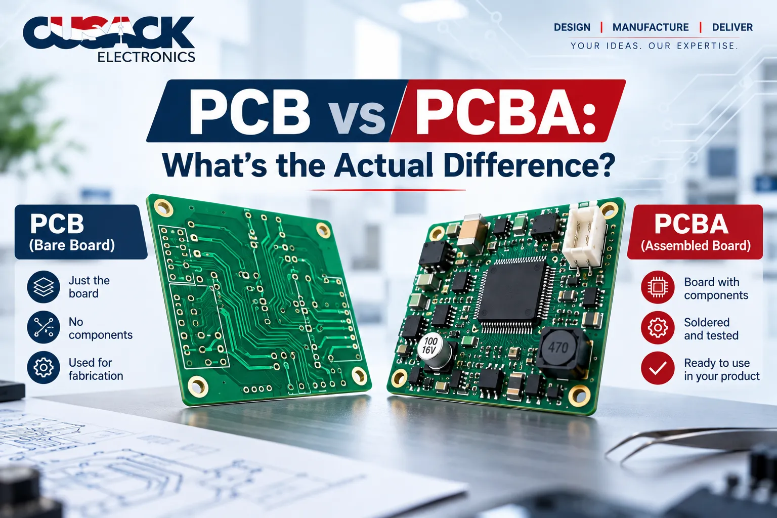
- PCB vs PCBA comes down to one question: are the parts on it yet? A PCB is the bare board. A PCBA is that same board with electronic components soldered on.
- A PCB cannot do anything by itself. It routes signals through copper, but nothing happens until components are attached.
- A PCBA is a working circuit. Power it up, and it performs a function.
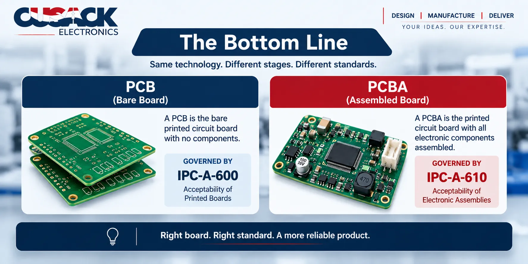
- The industry’s own standards body splits them into two. IPC judges bare boards under IPC-A-600 and finished assemblies under IPC-A-610.
- Which one you order is a purchasing decision, not a vocabulary quiz. Get it wrong, and you lose weeks.
PCB vs PCBA is one of the first distinctions anyone building hardware has to get straight. The two terms differ by a single letter, and that letter separates a slab of copper and fiberglass from a working circuit.
Here is my take before the definitions: the label matters less than the purchasing decision behind it. Ordering bare boards when you needed working ones, or paying for assembly you could have done at your bench, is an easy way to lose a few weeks.
What Is the Difference Between PCB and PCBA?
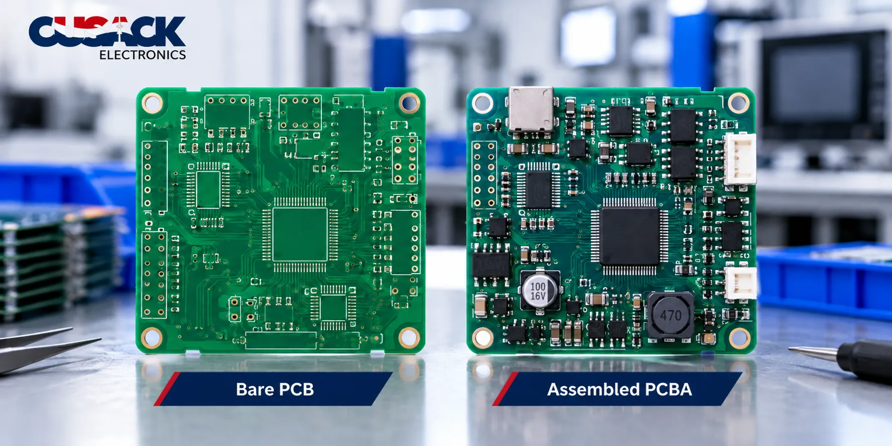
A PCB (printed circuit board) is the bare board: layers of insulating material and copper that route electrical signals but do nothing on their own. A PCBA (printed circuit board assembly) is that same board after electronic components have been soldered on, turning it into a working circuit.
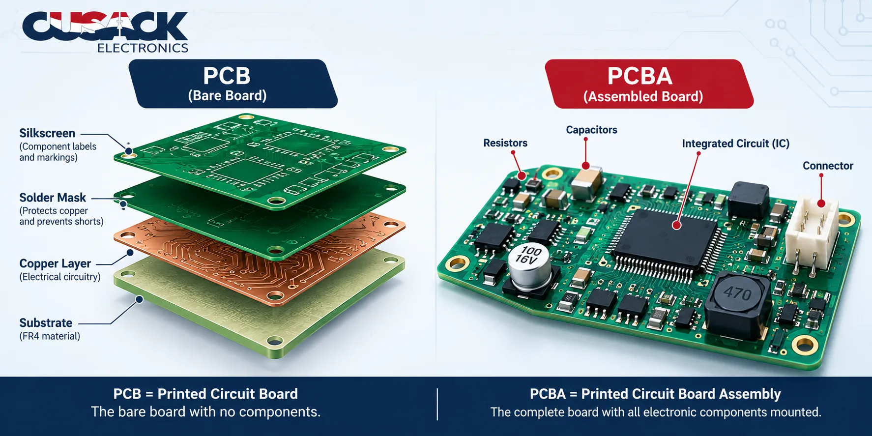
Picture a new house with the wiring run through the walls and nothing connected. Every circuit exists, yet flipping a switch does nothing, because there is no switch. That house is the PCB. Install the outlets, fixtures, and breaker panel, and you have the PCBA.
What Is a PCB?
A printed circuit board is a rigid or flexible board that supports components and connects them electrically through copper traces. It is built in layers:
- Substrate: the insulating core, most often FR-4, a glass-reinforced epoxy laminate
- Copper: etched into traces and pads that carry signals and power
- Solder mask: the coating, usually green, that keeps solder where it belongs
- Silkscreen: the printed labels you read on the surface
Simple boards have two copper layers; dense designs stack twelve or more. The substrate choice changes how a board handles heat and high-frequency signals, which I cover in my breakdown of PCB materials and board types.
What a PCB does not have is any function. It is a map of connections waiting for parts.
What Is a PCBA?
A printed circuit board assembly is a PCB with its electronic components mounted and soldered in place. The PCBA meaning covers two things in practice: the finished populated board, and the process of building it, also called PCB assembly.
Once resistors, capacitors, integrated circuits, and connectors are soldered on, the board can do its job, whether that is regulating power, reading a sensor, or running firmware.
This is where most of the value sits. PCB assembly was the largest single service segment in the US electronics manufacturing services market in 2025, according to Mordor Intelligence.
That July 2026 report put its share at 48.29%.
PCB vs PCBA Comparison: How Do They Differ Side by Side?
The difference between a PCB and a PCBA shows up in almost every attribute a buyer cares about, from what you send the supplier to how the result is inspected.
| PCB (bare board) | PCBA (assembled board) | |
|---|---|---|
| What it is | Board with copper traces, no parts | Board with components soldered on |
| Function | None on its own | Performs its designed function |
| Manufacturing stage | Fabrication | Assembly |
| Main processes | Imaging, etching, drilling, plating | Solder paste printing, placement, reflow, through-hole soldering |
| IPC acceptance standard | IPC-A-600 | IPC-A-610 |
| Typical testing | Electrical test for opens and shorts | Optical and X-ray inspection, in-circuit and functional test |
| Files you supply | Gerber files, drill files, fabrication drawing | All of those, plus bill of materials, pick-and-place file, assembly drawing |
| Biggest cost driver | Layer count, board size, materials | Component cost |
If you only remember one row, make it the files row. An assembly order needs everything about the board plus everything about the parts that go on it. I walk through that full handoff in my guide to electronic contract manufacturing.
Why Does IPC Treat a Bare Board and an Assembly as Separate Things?
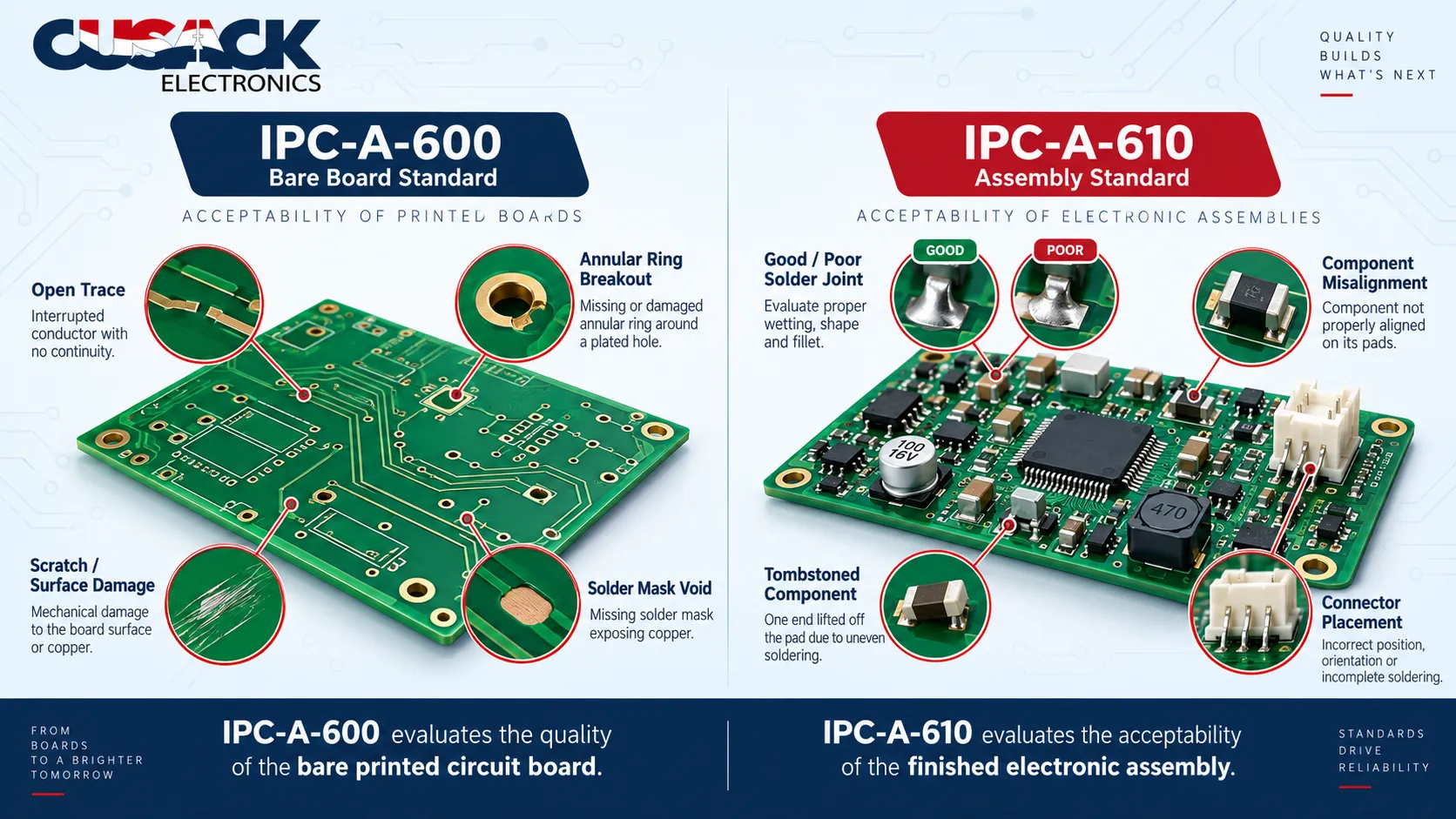
IPC, the industry association that writes electronics manufacturing standards, publishes two separate acceptance standards: one for bare boards and one for assemblies. That split is the most authoritative answer to the difference between PCB and PCBA you will find.
- IPC-A-600 covers bare printed boards. The current revision, IPC-A-600M, was published in 2025, superseding IPC-A-600K from 2020. It judges flaws inside the board: plating voids, annular ring registration, conductor thickness.
- IPC-A-610 covers electronic assemblies. It sets the acceptance requirements for electronic assemblies, judging solder joints, component placement, and orientation.
One document asks whether the board was made correctly. The other asks whether the parts were attached correctly.
That matters when you buy a PCBA. The board underneath is still judged against IPC-A-600 and its companion specification, IPC-6012. A flawless solder joint on a board with a hidden plating void is still a failure waiting to happen.
How Does a Bare Board Become a PCBA?
A bare board becomes a PCBA through the PCB assembly process: solder paste goes on, parts are placed, the solder is melted into joints, and the result is inspected. Surface-mount technology (SMT) handles most of it.
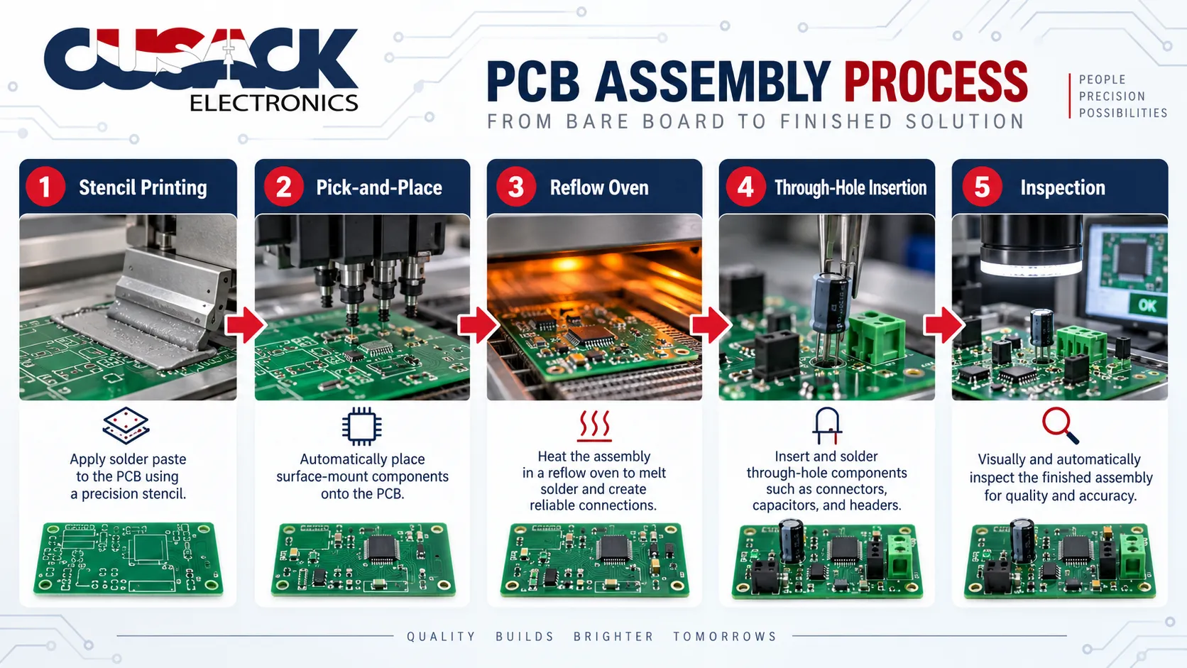
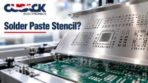
- Solder paste printing. A steel stencil lays solder paste, tiny solder spheres suspended in flux, onto every pad. It works like frosting a cake through a stencil: paste lands only where the openings are.
- Component placement. A pick-and-place machine lifts surface-mount devices (SMDs) off reels and sets each one on its pads. The tacky paste holds them.
- Reflow soldering. The board passes through an oven on a controlled temperature profile. The paste melts, wets the leads, then cools into permanent joints.
- Through-hole assembly. Parts with wire leads, like connectors, go through drilled holes. Through-hole technology (THT) joints are made by wave soldering, selective soldering, or by hand.
- Inspection and testing. Cameras check placement, X-ray looks beneath hidden joints, and electrical tests confirm the board works.
Most boards use both methods. SMT is fast and dense. Through-hole technology survives mechanical stress better, which is why a connector you plug in daily usually goes through the board rather than sitting on it.
I cover each stage, including the defects each one tends to produce, in my complete guide to PCB assembly.
Bare Board vs Assembled: How Is Each One Tested?
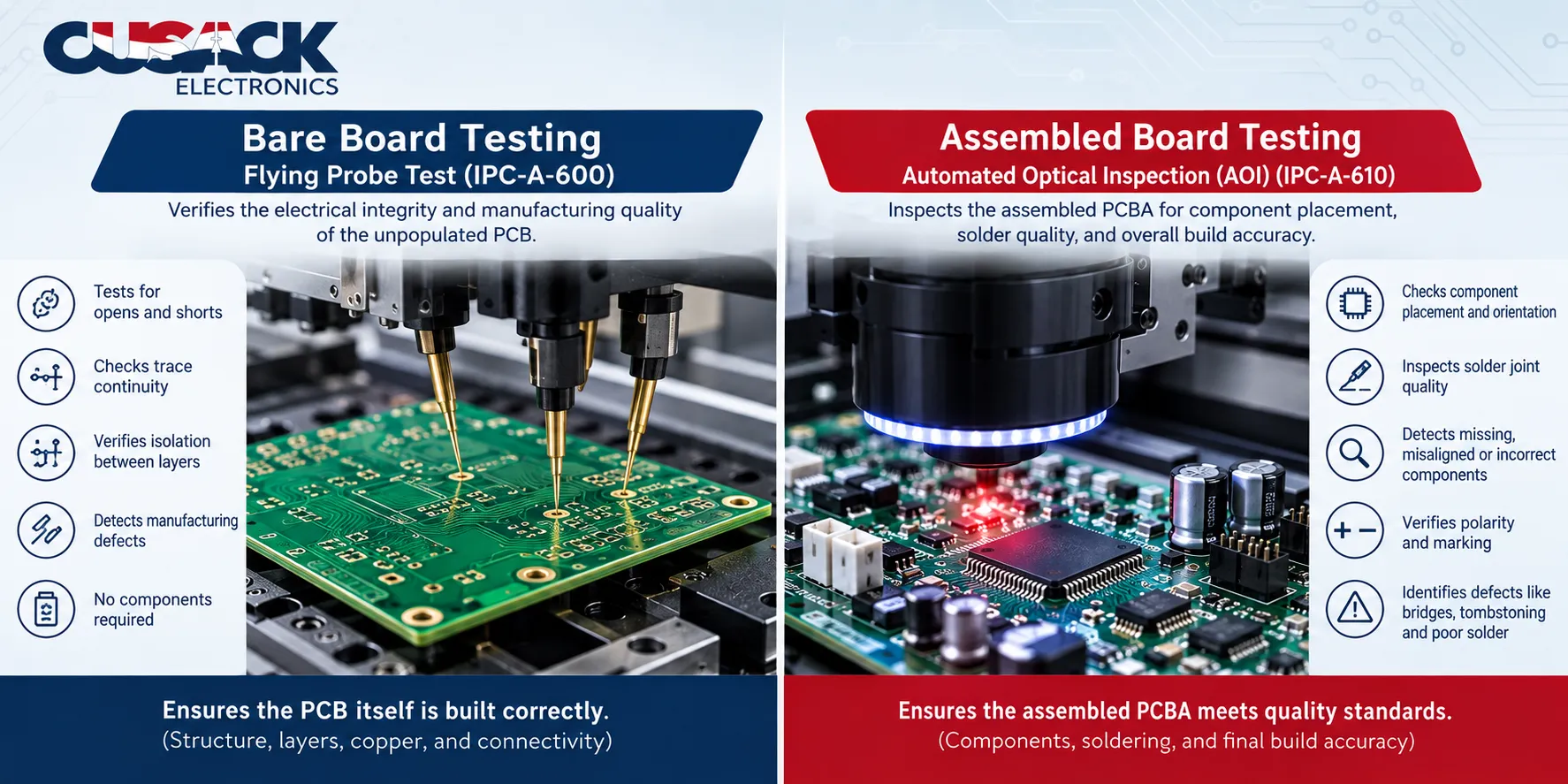
Bare boards and assembled boards are tested for completely different failures. Bare board vs assembled testing is where buyers often assume one check covers both, and it does not.
A bare board gets an electrical test comparing the copper against the design netlist, checking for opens (broken connections) and shorts (connections that should not exist).
That test uses either a flying probe, where moving probes need no custom fixture, or a bed-of-nails fixture that tests every point at once and suits volume.
An assembled board gets a layered set of checks:
- Automated optical inspection (AOI): cameras compare each part and joint against the expected image
- X-ray inspection: sees joints hidden under packages such as ball grid arrays
- In-circuit test (ICT): confirms component values and connections
- Functional test: powers the board up and confirms it does its job
Here is the part people miss. A bare board test proves the roads were built correctly, but it tells you nothing about the traffic. A board can pass every fabrication test and still fail after assembly.
The full range of methods is in my guide to PCB testing and inspection methods.
Should You Order a PCB or a PCBA?
Order bare PCBs when you or someone else will attach the parts. Order a PCBA when you need working boards from one supplier.
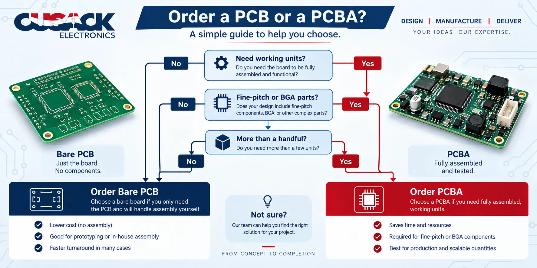
Order bare boards if:
- You are hand-soldering a few prototypes to test a concept
- You already have an assembly partner or an in-house line
- You want to confirm the fabrication before committing to expensive parts
Order a PCBA if:
- You need functioning units, not a kit of parts
- The design uses fine-pitch packages or ball grid arrays that cannot be reliably hand-soldered
- You are past a handful of units and consistency matters
Honest caveat: hand-assembling your own boards is a real skill, and for a first spin it is often cheaper. It stops making sense the moment a ball grid array appears on the bill of materials, because you cannot inspect a joint you cannot see.
Why Does a PCBA Cost So Much More Than a PCB?
A PCBA costs more because you are paying for the parts and the process of attaching them, and the parts usually dominate. A single microcontroller can cost more than the board it sits on.
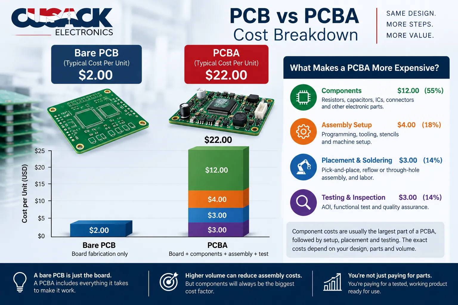
- Components: typically the largest line item, and the most exposed to shortages
- Setup: stencil, machine programming, and first-article inspection, spread across the run
- Complexity: more parts, double-sided assembly, and mixed SMT and through-hole all add passes
- Testing depth: fixtures and X-ray add cost that pays for itself in escaped defects
Volume changes everything. A batch of 25 carries a per-unit setup cost that barely registers at 2,500.
The quote mechanics are in my breakdown of what drives PCB assembly cost. Whether you or the assembler buys the parts is covered in this comparison of turnkey and consignment assembly.
The Bottom Line
A PCB is the board. A PCBA is the board with its electronic components soldered on and working. The processes, standards, tests, and costs all follow from that one difference.
If you are unsure which to order, ask whether you want to hold a working circuit when the box arrives. If yes, you want a PCBA.
Need boards built rather than just fabricated? Send me your Gerber files and bill of materials and I will come back with a quote and a straight answer on whether assembly makes sense at your volume. Request a quote here.
Frequently Asked Questions
Is PCBA the same as PCB assembly?
Mostly, yes. PCB assembly usually names the process of mounting and soldering components onto a board, while PCBA names both that process and the finished product. A supplier quoting PCBA means a populated, soldered board. An engineer saying the PCBA failed means the physical board.
Is a PCB the same as a circuit board?
In everyday use, yes. Circuit board is the general term, and PCB is the specific name for a board with printed copper traces, which covers nearly every modern device. You may also see PWB, printed wiring board, an older term some engineers still use to signal that nothing is mounted yet.
What is the difference between SMD and SMT?
SMD, surface-mount device, is the component itself, designed to sit on the board surface. SMT, surface-mount technology, is the method of attaching it: solder paste, pick-and-place machines, and reflow. You place SMDs using SMT, the same way you drive screws using a screwdriver.
Can I turn a PCB into a PCBA myself?
Yes, for many designs. Through-hole parts and larger surface-mount packages can be soldered by hand with a good iron, flux, and practice. Fine-pitch chips and ball grid arrays are different, because their joints need controlled reflow and usually X-ray inspection to verify.
Why does a PCBA take longer to deliver than a PCB?
A PCBA needs everything a bare board needs plus component sourcing, stencil preparation, assembly, and testing. Component availability usually decides the timeline, since one part on a long lead time holds up the whole build. Sharing your bill of materials early lets the assembler flag slow parts first.
Does a PCBA include the enclosure and cables?
No. A PCBA stops at the populated board. Putting it into a housing with cables and displays is a separate step called box build, which turns an assembly into a finished product. The steps are in my overview of the box-build assembly process.