TL;DR: Wave soldering pumps molten solder into a standing wave and passes a circuit board over it, forming every through-hole solder joint on the underside in one sweep. It runs in four stages: flux, preheat, wave contact, cooling. It is still the fastest and cheapest way to solder a lot of leaded pins, and it is also the dirtiest process on most assembly floors. If your board carries only a handful of leaded parts, selective soldering or paste-in-hole will serve you better.
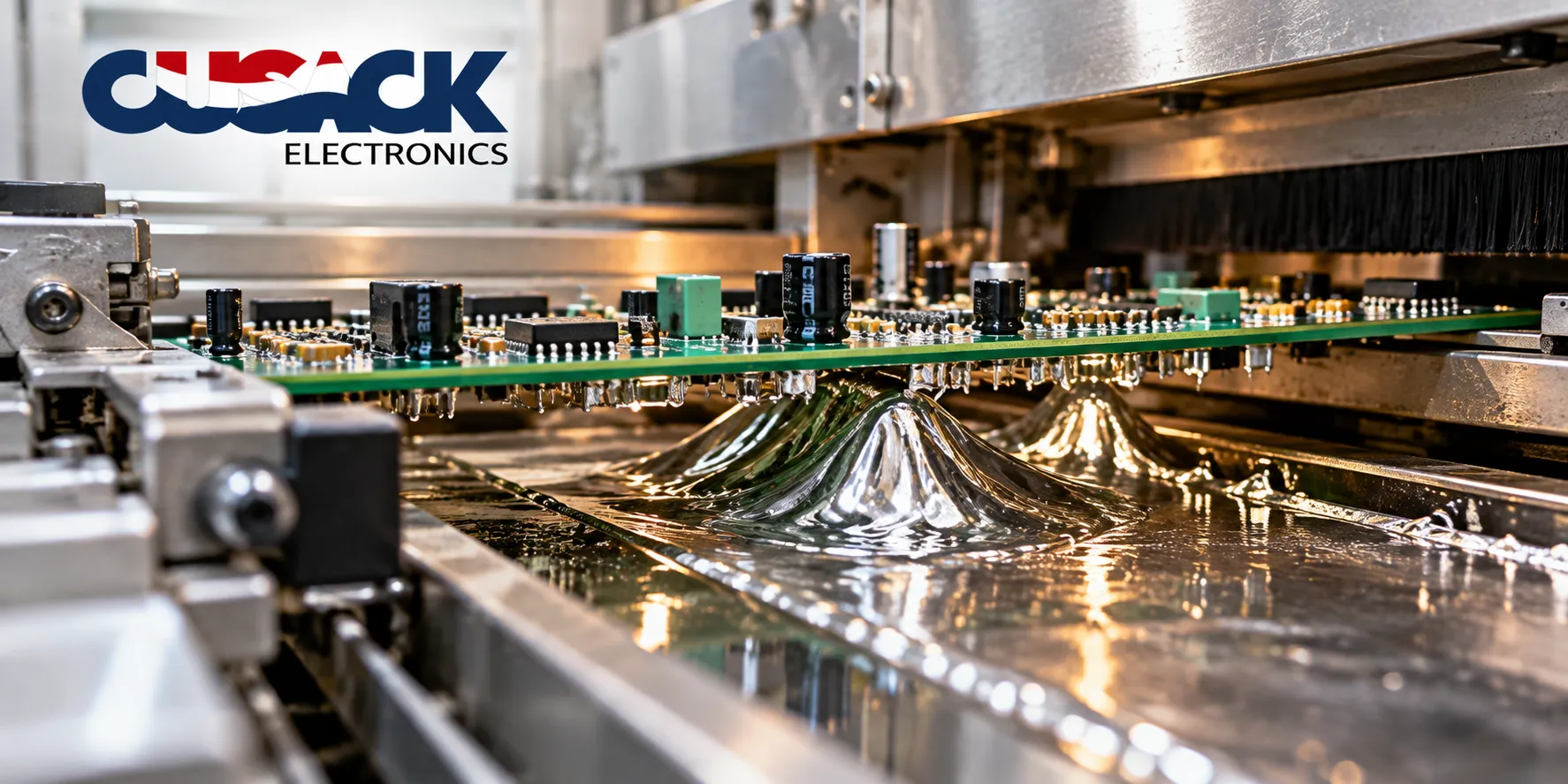
This is the oldest automated process still running on a modern assembly floor, and most of what gets written about it skips the part that matters to whoever pays for it.
Here is my flat opinion. The process earns its place on exactly one kind of board: high volume, lots of through-hole pins, and a design that tolerates the whole underside being dipped in molten metal. On anything else it is a liability you are paying to maintain.
That is not a popular position for a contract manufacturer to take, because the cost per joint is low once the machine is warm. But the cost of a wave line is not the cost per joint, and I will show you the numbers that make that case.
What Is Wave Soldering?
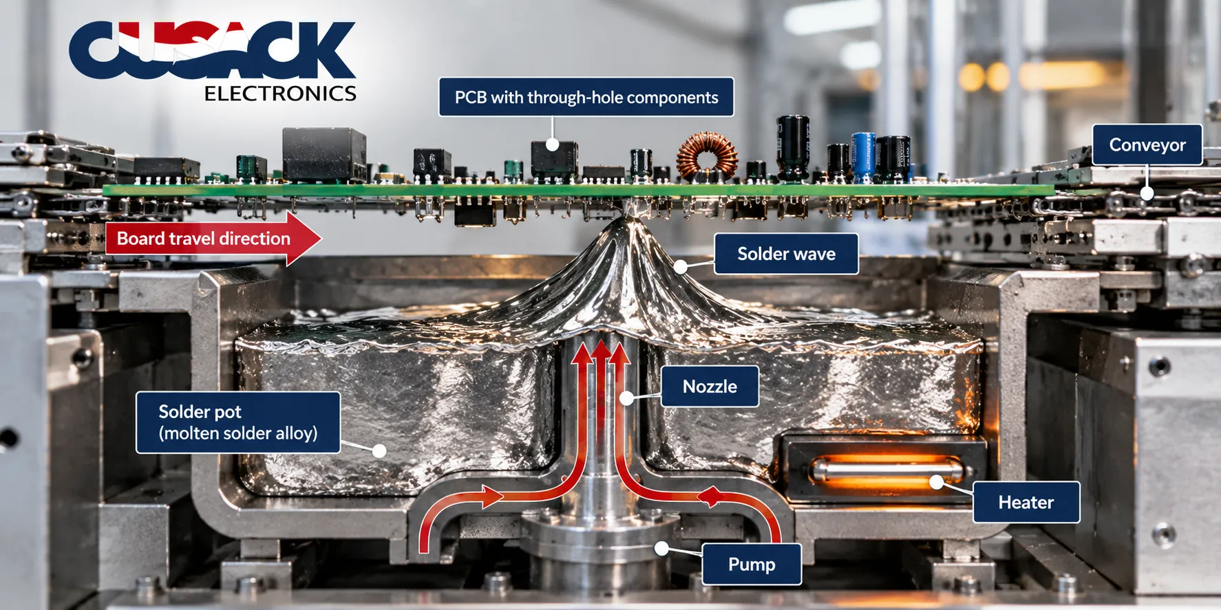
Wave soldering is a bulk soldering process that solders every exposed joint on the underside of a printed circuit board at once, by passing the board across a standing wave of molten solder.
Picture a fountain of liquid metal. A pump in the solder pot forces molten alloy up through a nozzle so it forms a continuous crest, and a conveyor system carries the board across that crest at a fixed speed and angle.
Wikipedia describes it as the board passing over molten solder where a pump creates an upwelling resembling a standing wave. That is exactly what it looks like on the floor.
The key word is bulk. The machine does not choose which joints to make. Every piece of exposed metal that touches the solder wave gets soldered, which is the source of both its speed and its problems.
That makes it the counterpart of through-hole technology (THT), the older method where component leads pass through drilled holes rather than sitting on surface pads.
How Wave Soldering Works, Stage by Stage
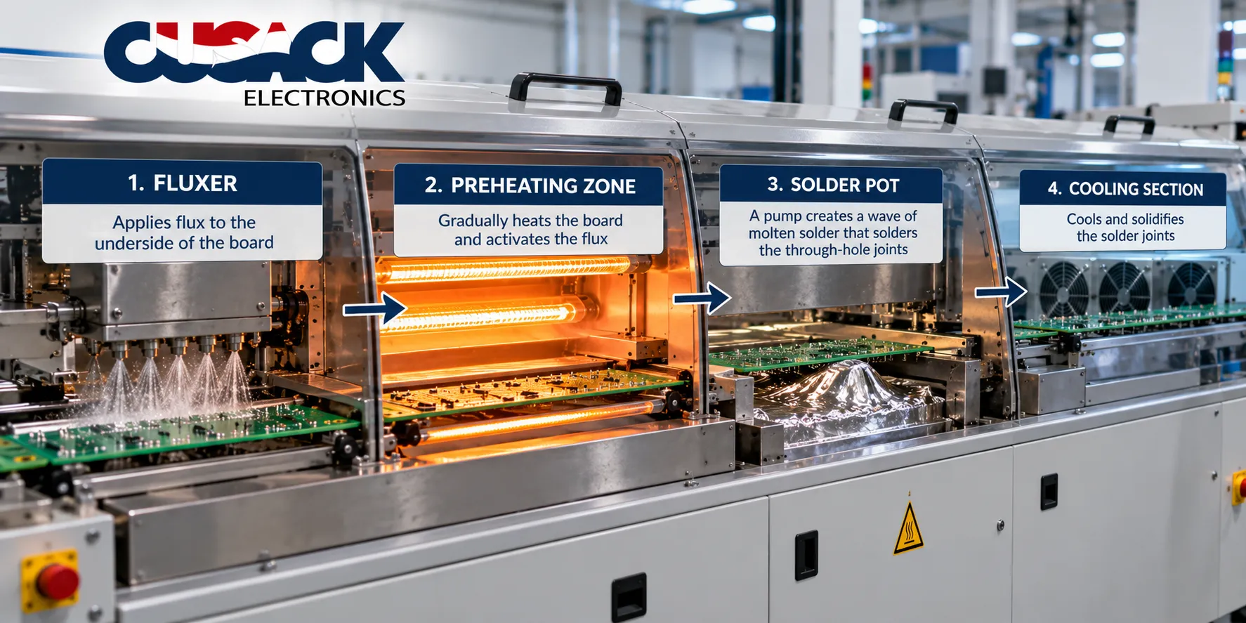
The short answer on how wave soldering works is four stages, and the board passes through all of them on one continuous conveyor system.
Flux Application
Flux is applied to the underside of the board first, usually by spray, to strip oxide off the pads and component leads so the alloy can wet them.
Without flux, molten metal simply beads off an oxidised surface, the way water beads on a waxed car. The flux removes that barrier for the few seconds it is needed.
Most electronic assembly now runs no-clean flux with a solids content in the low single digits by percentage. Low solids means less residue left behind, but also less margin, because there is less active chemistry to survive preheat.
Preheating Zone
The preheating zone raises board temperature before it meets the crest, typically into the range of about 100 to 150 degrees Celsius measured on the top surface.
Preheat does two jobs. It activates the flux and drives off its solvent carrier, and it narrows the temperature gap between the board and the pot so the board does not take a thermal shock on contact.
Skip it and you get cracked ceramic parts and lifted pads. Overdo it and the flux is spent before the joint is formed.
The Solder Wave
The solder wave is the contact point, where molten alloy wets the lead and the plated hole, then draws up into the barrel by capillary action.
Contact time is short. Wikipedia puts the typical dwell at two to four seconds, governed by conveyor speed and wave height, and that is the single most adjusted parameter on the machine.
The pot runs hot, generally around 250 to 260 degrees Celsius for lead-free alloys, well above melting point so the metal stays fluid across the whole crest.
The conveyor also runs on a slight incline, a few degrees, so the board peels away rather than lifting off flat. That peel angle drains excess solder back into the pot instead of leaving it bridged across adjacent pins.
Cooling
Cooling brings the board down at a controlled rate so each solder joint solidifies with a sound grain structure and the laminate does not warp.
Too fast and you stress the board and the joints. Too slow and you keep everything hot long enough to grow brittle intermetallic layers. Forced air is the usual method.
Single Wave, Dual Wave, or Selective Pallets?
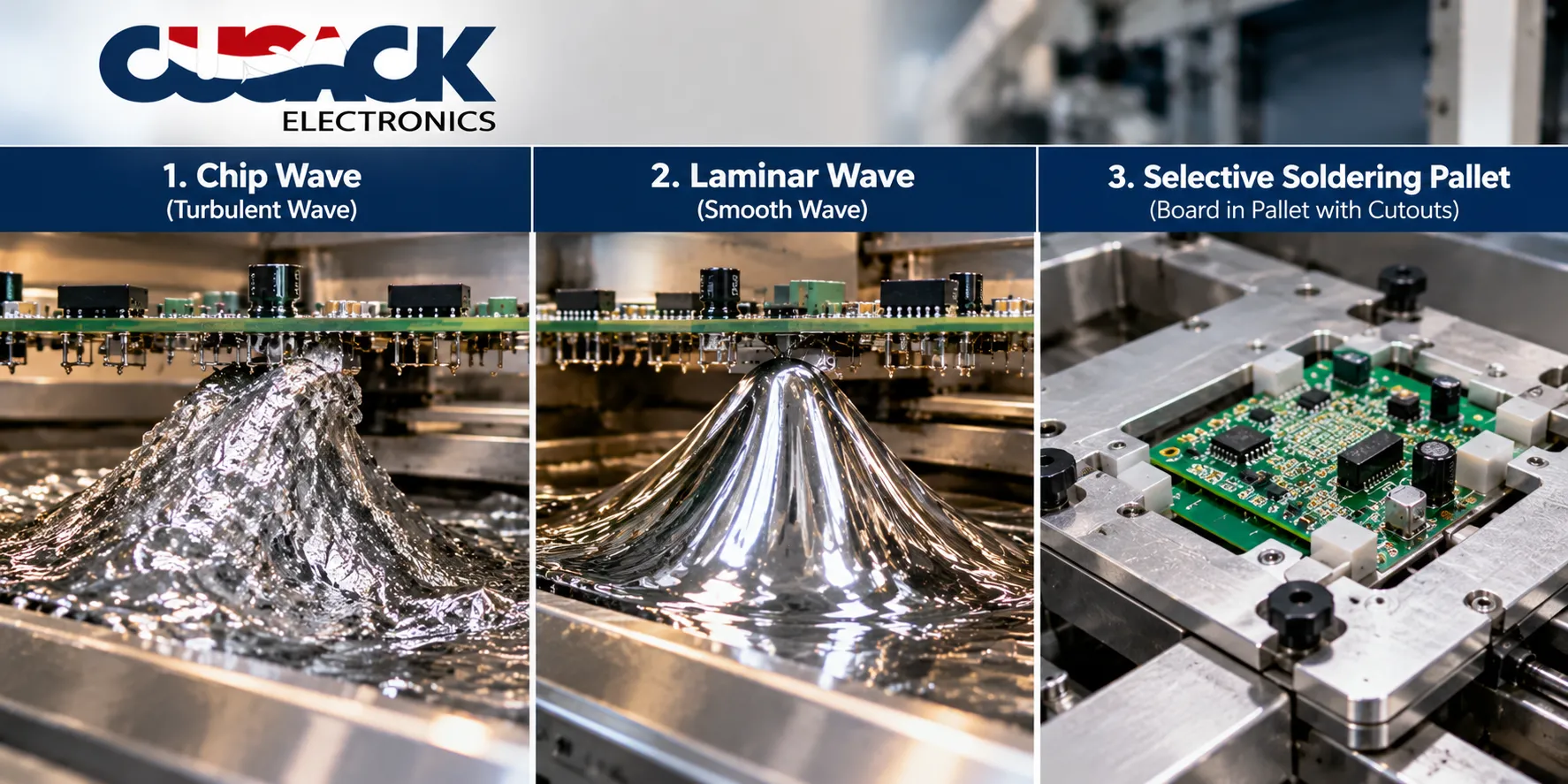
Machines come in three configurations, and which one you need is decided by what sits on the underside of the board.
- Single wave: one smooth, laminar crest. Fine where all the through-hole components sit on a clear underside with nothing else in the way.
- Dual wave: a turbulent first crest followed by a smooth second one. The turbulent one, often called a chip wave, forces alloy into shadowed areas behind surface-mount parts glued underneath; the laminar one then clears bridges the first left behind.
- Selective pallet: a machined carrier that masks the board and exposes only the joints you want made. This is how a mixed board goes through without the surface-mount side being wrecked.
Wikipedia notes that operators choose between smooth laminar crests and higher-pressure turbulent ones depending on the board.
Pallets are the honest tell. The moment your board needs machined tooling to survive the process, you are paying for that tooling, its storage, and a setup step, and the economics that made this attractive start to erode.
Which Parameters Actually Matter?
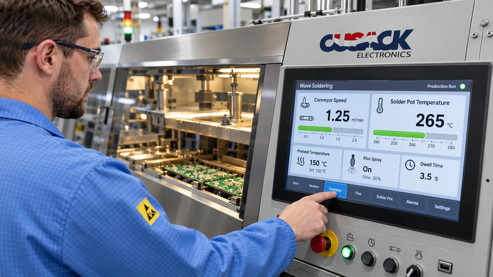
Treat the table below as typical operating windows, not as settings to copy. Your real numbers come from the flux and alloy supplier, and from profiling the board itself.
| Parameter | Typical window | What it controls |
|---|---|---|
| Flux solids content | Low single digit percent | How much active chemistry survives to the crest |
| Topside preheat | About 100 to 150 degrees C | Flux activation and thermal shock margin |
| Solder pot temperature | About 250 to 260 degrees C, lead-free | Fluidity and wetting speed |
| Contact time | 2 to 4 seconds | Hole fill versus heat damage |
| Conveyor speed | Set to hit the contact time | Everything else, all at once |
| Conveyor angle | A few degrees of incline | Drainage and bridging |
| Nitrogen level | Measured in parts per million oxygen | Dross formation and wetting quality |
The same standard that governs reflow profiling covers this side too. IPC-7530B, Guidelines for Temperature Profiling for Mass Soldering Processes, Reflow and Wave, was published in 2025 and replaced the 2017 A revision.
Conveyor speed is the parameter people reach for first and should reach for last. It changes contact time, preheat exposure, and cooling rate at once, so a speed change to fix bridging quietly alters two other things.
Nitrogen is the one worth explaining, because it is a running cost rather than a setting. Flooding the pot area with nitrogen displaces oxygen, which cuts dross formation sharply and improves wetting.
The catch is that nitrogen costs money every hour the line runs, so it earns its place on fine-pitch or high-volume work and rarely on anything else.
What Makes a Board Wave-Friendly?
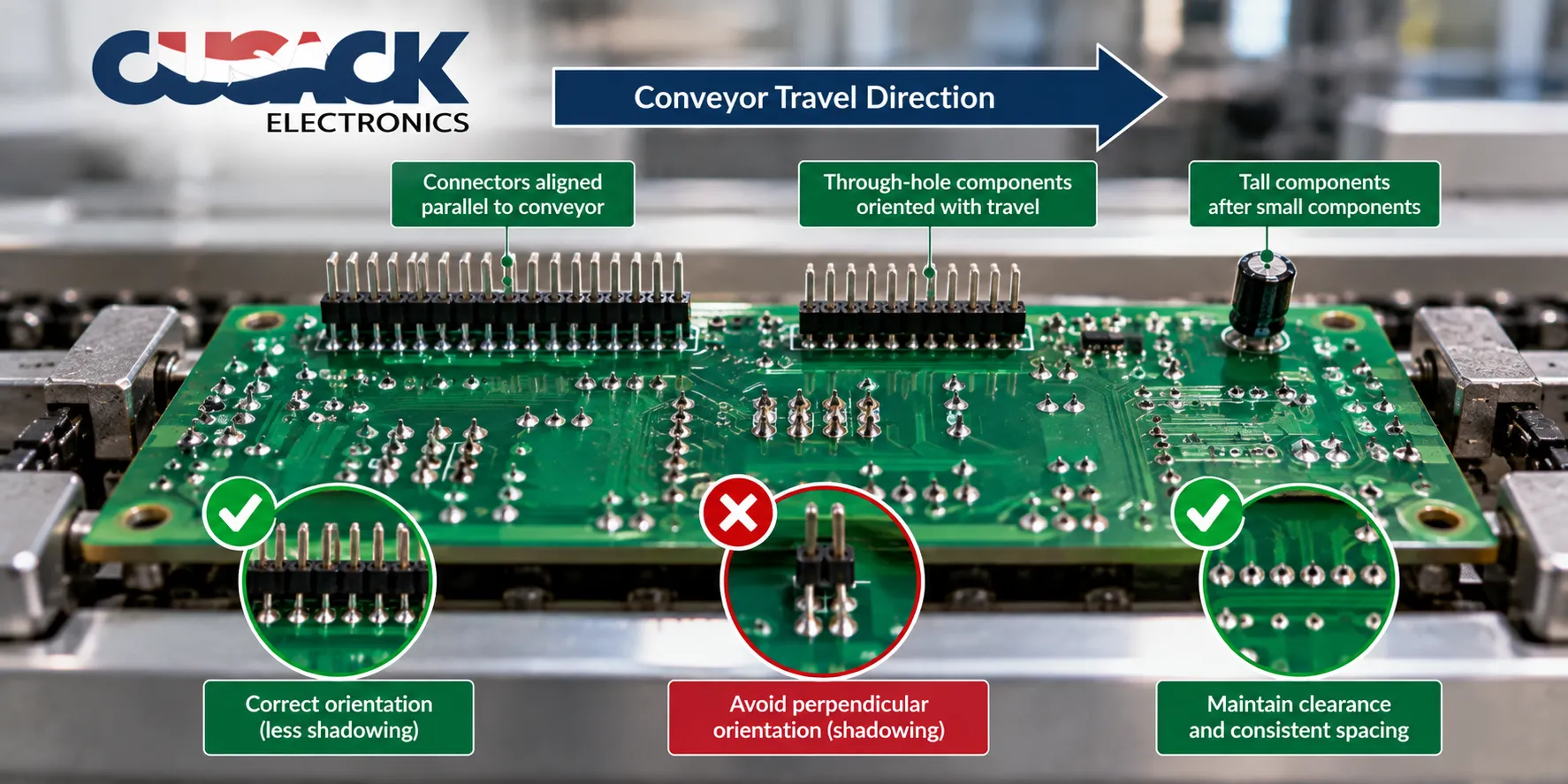
Design decides most of your defect rate here, and the choices get locked long before anyone switches a machine on.
- Orient connectors along the travel direction. A row of pins presented in line drains cleanly. The same row turned across the direction of travel sits in its own shadow and bridges.
- Put thermal relief on pads tied to a plane. A pad connected straight into a large copper pour wicks heat away faster than the crest can deliver it, and the hole never fills. Spoke connections solve it.
- Keep the underside clear. Every surface-mount part down there forces you into a dual crest or a pallet, and both cost money.
- Watch lead protrusion. Leads that stick out too far catch and bridge; too short and you cannot confirm fill. IPC gives an acceptable range, commonly cited as roughly 0.7 to 2.5 millimetres.
- Leave a shadow gap behind tall parts. Anything standing proud shields what sits downstream of it.
None of that is expensive to do at layout stage. All of it is expensive to discover at first article.
Wave Soldering vs Reflow Soldering
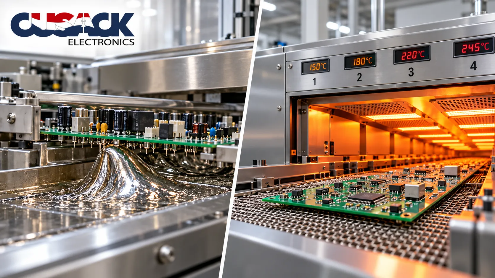
The wave vs. reflow question comes down to where the solder comes from. One supplies molten alloy from a pot at the moment of contact. The other melts paste that was already printed onto the pads before the parts went on.
| Wave | Reflow | |
|---|---|---|
| Solder source | Molten pot, applied at contact | Paste printed before placement |
| Joints formed | Everything exposed on the underside | Only where paste was printed |
| Suits | Through-hole components (THT) | Surface-mount devices (SMT) |
| Selectivity | None without a pallet | Inherent, set by the stencil |
| Thermal exposure | Seconds, one side | Minutes, whole board |
| Dross and maintenance | High | None |
They are not really rivals. Almost every board uses both: reflow first for the surface-mount side, then the pot for the leaded parts that follow.
For the reflow side properly, including the four profile zones and how to build a profile for a specific board, see my guide to reflow soldering. The two underlying technologies are compared in SMT vs. through-hole.
Selective Soldering vs Wave Soldering
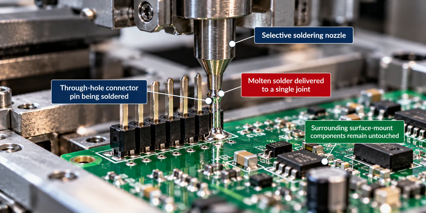
Selective soldering does the same physical job through a nozzle a few millimetres across, moving under computer control to treat one joint or one connector at a time.
Think of the bulk process as painting a wall with a roller and selective soldering as using a brush. The roller is faster across a big flat area. The brush is the only option when most of the wall must stay clean.
The trade is throughput against flexibility, and the numbers are stark.
In a study by David Geiger and Murad Kurwa of Flex, the bulk process ran at more than 15 pins per second against roughly 8 for selective.
Cost per unit told the same story. In their model of 100,000 units a year at 1,000 pins each, the pot came out cheapest by a wide margin, with selective several times more expensive per unit.
So why would anyone choose the slower, dearer option? Because of what the same study found about dross.
Is Wave Soldering Still Worth It?
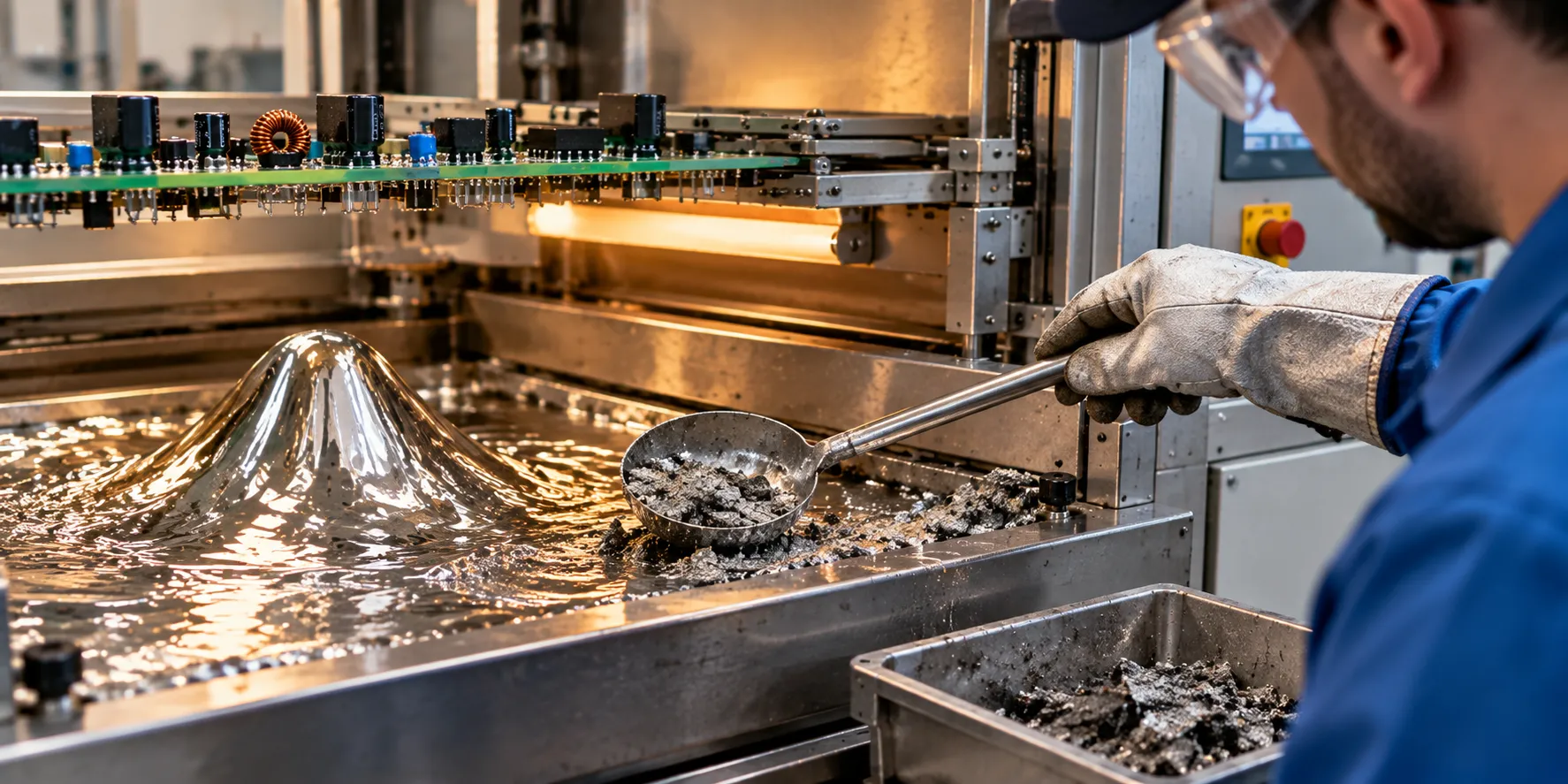
Wave soldering is still worth it on high-volume, through-hole-heavy boards, and increasingly hard to justify on anything else. The reason is not joint quality. It is everything around the pot.
Dross is the oxide skin that forms on molten alloy and has to be skimmed off. The Flex study measured wave lines producing 3 to 26 kilograms of it every 24 hours, against 0.2 to 0.5 kilograms for selective.
That is not a rounding difference. It is scrapped alloy, operator time, and a recurring hazardous task. The same authors describe pot maintenance as one of the dirtiest and most hazardous processes on a production floor, between the fumes, the dross dust, and the molten metal.
Their recommended order of preference is worth sitting with, because it comes from a company running assembly at enormous scale: paste-in-hole first, then robotic point soldering, then selective, and the wave last.
Paste-in-hole is the one people forget. You print extra paste into the plated holes during the normal stencil step, place the leaded part, and let the reflow oven do the work. No second machine, no pot, no dross.
It does not fit every part, because the component has to survive a full reflow profile, and plenty of connectors cannot.
When it does fit, though, it removes a whole process step. Whether it fits is a design question, which is why it belongs in a design for manufacturability review rather than a production meeting.
My honest caveat: if you are building tens of thousands of boards a year with a hundred or more leaded pins on each, the wave still wins on cost, and nothing here changes that.
What Goes Wrong? In wave soldering
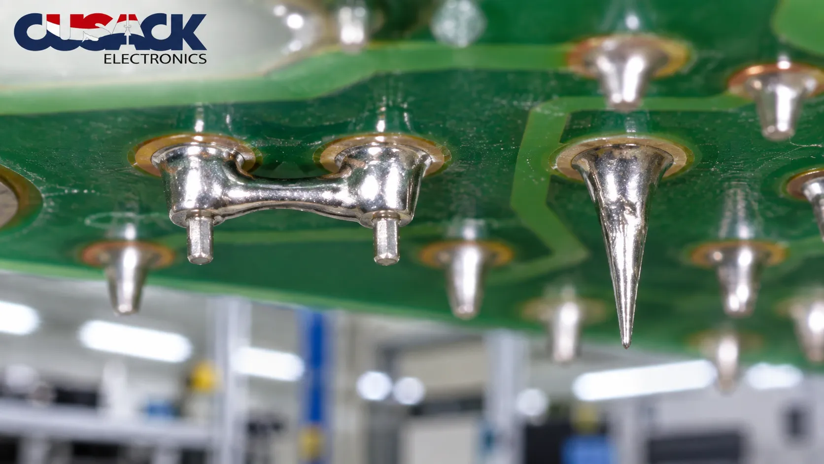
Most defects here trace back to one of four things: flux, preheat, contact time, or the way the board leaves the crest.
| Defect | What you see | Usual cause |
|---|---|---|
| Bridging | Alloy joining adjacent pins | Conveyor too fast, wrong peel angle, or pad spacing too tight |
| Icicles | Spikes hanging off leads | Poor drainage on exit, or pot temperature too low |
| Insufficient hole fill | Metal not drawn up the barrel | Contact time too short, preheat too low, or spent flux |
| Dewetting | Solder pulls back off a pad | Contaminated surface or inadequate flux coverage |
| Solder balls | Beads stuck to the board surface | Trapped flux solvent flashing off, usually a preheat problem |
| Lifted pads | Copper pulled away from laminate | Excessive thermal shock on contact |
| Component cracking | Fractured ceramic bodies | Preheat skipped or ramped too steeply |
Notice how many come back to preheat and conveyor speed. Those two settings do most of the damage and most of the fixing.
Catching them is its own job, since these joints sit on the underside where a top-down camera cannot help. I have gone through the options in my guide to PCB testing methods.
Frequently Asked Questions
What is wave soldering used for?
It is used for through-hole assembly, where component leads pass through drilled holes in the board. It suits connectors, transformers, large capacitors, and anything mechanical, and it is most economical on high-volume boards carrying many leaded parts on a clear underside.
Can it be used on surface-mount boards?
Only indirectly. Surface-mount parts glued to the underside can be treated with a dual crest, and mixed boards go through on a selective pallet that masks the sensitive areas. Neither is ideal. Surface-mount joints are made properly by reflow, with the pot reserved for leaded parts.
What temperature does a wave soldering machine run at?
The solder pot typically sits around 250 to 260 degrees Celsius for lead-free alloys, with topside preheat somewhere near 100 to 150. The exact figures depend on your alloy and flux, and should come from the supplier datasheet rather than a general range.
How long does the board touch the crest?
Two to four seconds is the usual contact window, set by conveyor speed and wave height. Shorter and the metal may not draw fully up the plated hole; longer and you risk heat damage to the board and the parts on it.
Is wave soldering being phased out?
It is shrinking rather than disappearing. As through-hole technology content has fallen, the volumes that justify a dedicated line have thinned, and paste-in-hole and selective soldering now cover most low-count jobs. High-volume leaded work still runs on the wave, and will for a long while.
What is the difference between dross and slag?
Dross is the oxide layer that forms where molten alloy meets air in the pot, and it contains recoverable metal, so it is skimmed and often reclaimed. Slag is a general term for waste from a molten metal process. On an assembly floor you will hear dross almost exclusively.