A PCB assembly can look straightforward on the design screen but become complicated once production begins. Through-hole connectors, closely spaced surface-mount components, and limited board clearance can all affect the soldering process.
Selecting the right method helps manufacturers maintain reliable electrical connections while controlling production time and cost.
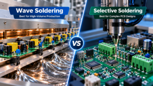
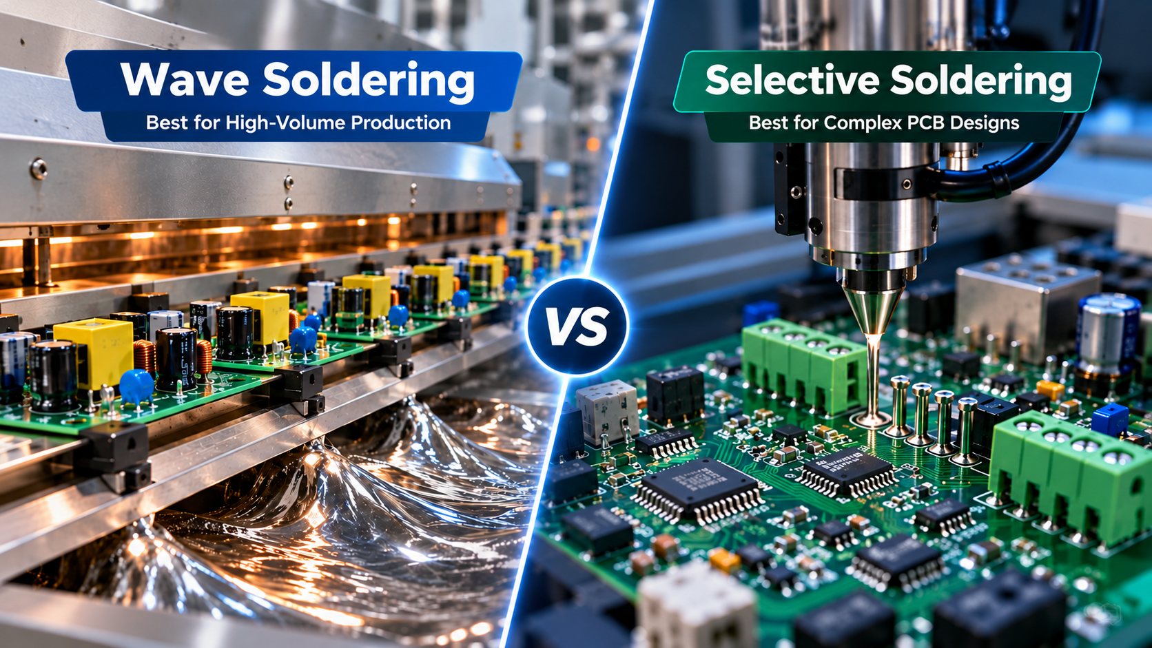
Selective soldering vs wave soldering is an important comparison for PCB designers and OEMs planning efficient assembly. Both methods create solder joints for through-hole components, but they differ in precision, production speed, equipment requirements, and suitability for complex circuit boards.
What Is Wave Soldering?
Wave soldering is an automated process that joins electronic components to printed circuit boards using a continuous wave of molten solder.
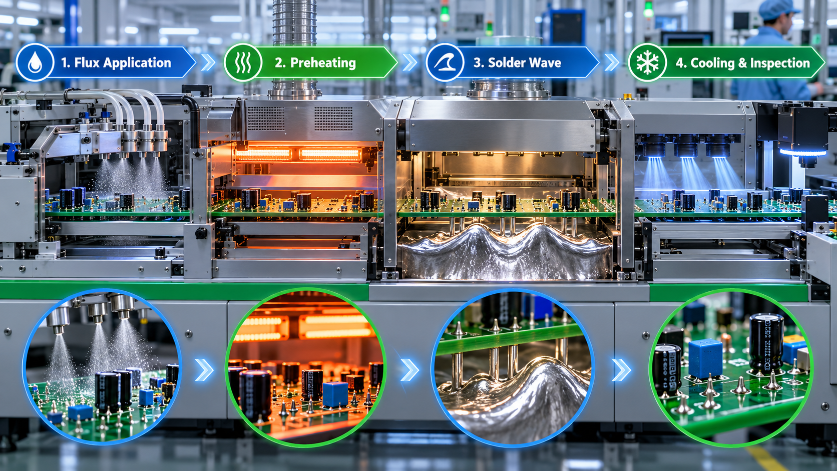
During production, the PCB travels through several stages:
- Flux application: Flux prepares exposed metal surfaces for soldering.
- Preheating: Controlled heating activates the flux and reduces thermal shock.
- Solder wave contact: The board passes over molten solder, allowing exposed component leads and pads to form connections.
- Cooling and inspection: The solder solidifies, and the assembly is checked for defects.
A wave soldering machine uses a conveyor system to move boards through these stages at controlled speeds.
This method is especially useful for high-volume production of PCBs with accessible through-hole components. However, boards containing densely packed or heat-sensitive components may require additional protection.
What Is Selective Soldering?
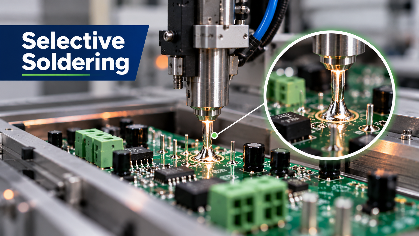
Selective soldering is a controlled process that applies molten solder only to designated areas of a PCB.
Instead of exposing a broad section of the board to a solder wave, programmable equipment directs a small solder fountain or nozzle toward specific joints.
The process generally includes localized flux application, preheating, and controlled solder contact.
This targeted approach is particularly useful for through hole soldering on assemblies containing both surface-mount and through-hole components.
For example, an industrial control board may contain surface-mounted microchips positioned close to large through-hole connectors. Selective soldering can form connections at those connectors without directly exposing surrounding areas to the solder wave.
Its main limitation is processing time. Soldering individual locations may take longer than processing an entire compatible board through a conventional wave soldering line.
Selective Soldering vs Wave Soldering: Key Differences
Both processes can produce reliable connections when matched with appropriate PCB designs and properly controlled manufacturing conditions.
Their major differences include solder application, production speed, equipment setup, and board compatibility.
| Feature | Selective Soldering | Wave Soldering |
| Solder application | Targets specific joints | Contacts a broader exposed area |
| Production speed | Depends on joint count and nozzle movement | Generally faster for compatible high-volume assemblies |
| PCB complexity | Suitable for dense, mixed-technology boards | Best for layouts designed for wave access |
| Heat exposure | More localized | Broader solder-wave exposure |
| Equipment setup | Requires programming and nozzle selection | Requires conveyor and soldering-profile setup |
| Cost efficiency | Useful for complex assemblies | Often economical for repetitive production |
The most suitable technique depends on component placement, production volume, and the physical accessibility of solder joints.
Advantages and Limitations of Each Soldering Method
Advantages and Limitations of Wave Soldering
Wave soldering offers efficient processing for circuit boards designed around automated solder-wave contact.
Its primary advantages include:
- Fast processing of compatible assemblies
- Repeatable soldering conditions
- Lower per-board processing costs at suitable production volumes
However, closely positioned surface-mount components, irregular component heights, and restricted clearances can make wave soldering difficult.
Additional masking fixtures may be necessary to prevent solder from reaching protected areas.
Advantages and Limitations of Selective Soldering
Selective soldering provides greater control over where molten solder contacts the PCB.
Its advantages include:
- Targeted soldering of through-hole connections
- Better compatibility with densely populated assemblies
- Reduced direct solder exposure for nearby components
Nevertheless, the method requires careful programming, sufficient nozzle access, and appropriate thermal settings.
Complex assemblies with numerous through-hole joints may also require longer processing cycles.
Neither method automatically guarantees better solder quality. Proper process control remains essential.
Which Soldering Method Is Better for Your PCB Assembly?
The right choice depends on the board’s design and manufacturing requirements.
Choose Wave Soldering for High-Volume Production
Wave soldering may be appropriate for products containing numerous accessible through-hole components.
Consider a power supply PCB with relatively open component spacing and a consistent design used across thousands of units.
A properly configured wave soldering line can process these assemblies efficiently while maintaining repeatable solder connections.
Choose Selective Soldering for Complex PCB Designs
Selective soldering is often better suited to mixed-technology assemblies where through-hole components are located near sensitive surface-mount devices.
Consider an industrial controller containing microprocessors, small resistors, and through-hole terminal blocks.
Targeted soldering can help protect adjacent components while creating the required electrical connections.
This distinction also matters when evaluating SMT vs through hole assembly requirements, since many modern electronic products combine both technologies on a single circuit board.
How Do Soldering Methods Affect PCB Quality and Cost?
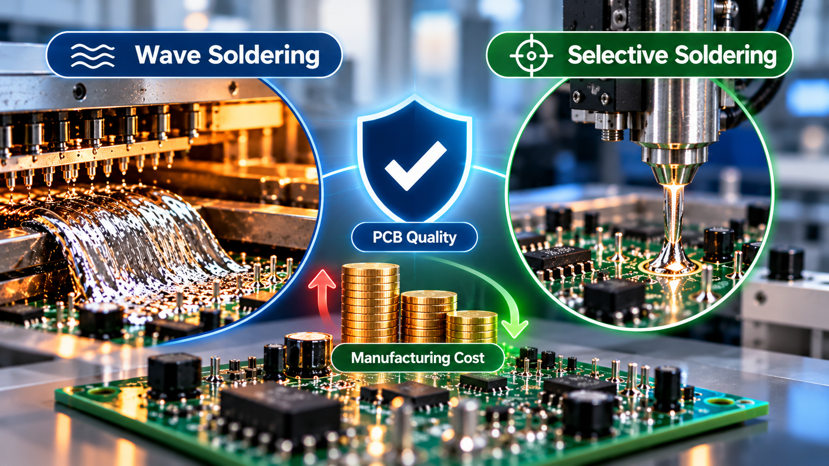
Wave soldering can reduce processing time for suitable production runs. However, poorly designed layouts or incorrect machine settings may contribute to solder bridges, insufficient hole fill, or other defects.
Selective soldering allows more localized process control, but programming, nozzle movement, and longer cycle times can increase manufacturing expenses.
Neither process eliminates the need for inspection and testing.
At Cusack Electronics, design-for-manufacturability reviews are part of the broader manufacturing process, helping identify assembly challenges before production.
Evaluating component placement, solder access, and testing requirements early can help reduce preventable manufacturing problems.
Frequently Asked Questions
Is selective soldering better than wave soldering?
Selective soldering is generally more suitable for complex or densely populated PCBs requiring targeted solder application. Wave soldering is often more efficient for high-volume assemblies designed for broad solder-wave contact.
Can wave soldering be used for SMT components?
Yes, certain surface-mount components can be wave soldered when the board and assembly process are specifically designed for it. However, reflow soldering is generally used for conventional SMT assembly.
Which soldering process is more cost-effective?
Wave soldering can provide lower processing costs for large production runs with compatible board layouts. Selective soldering may be more economical for complex assemblies where masking, manual soldering, or additional rework would otherwise increase costs.
Get Reliable PCB Assembly Support from Cusack Electronics
Choosing the right soldering approach begins with understanding the PCB’s component layout, performance requirements, and production volume.
Cusack Electronics supports OEMs with PCB assembly services, including SMT, through-hole, and mixed-technology assembly.
Need help planning a reliable, cost-effective PCB assembly process? Request a quote and discuss your project requirements with Cusack Electronics.