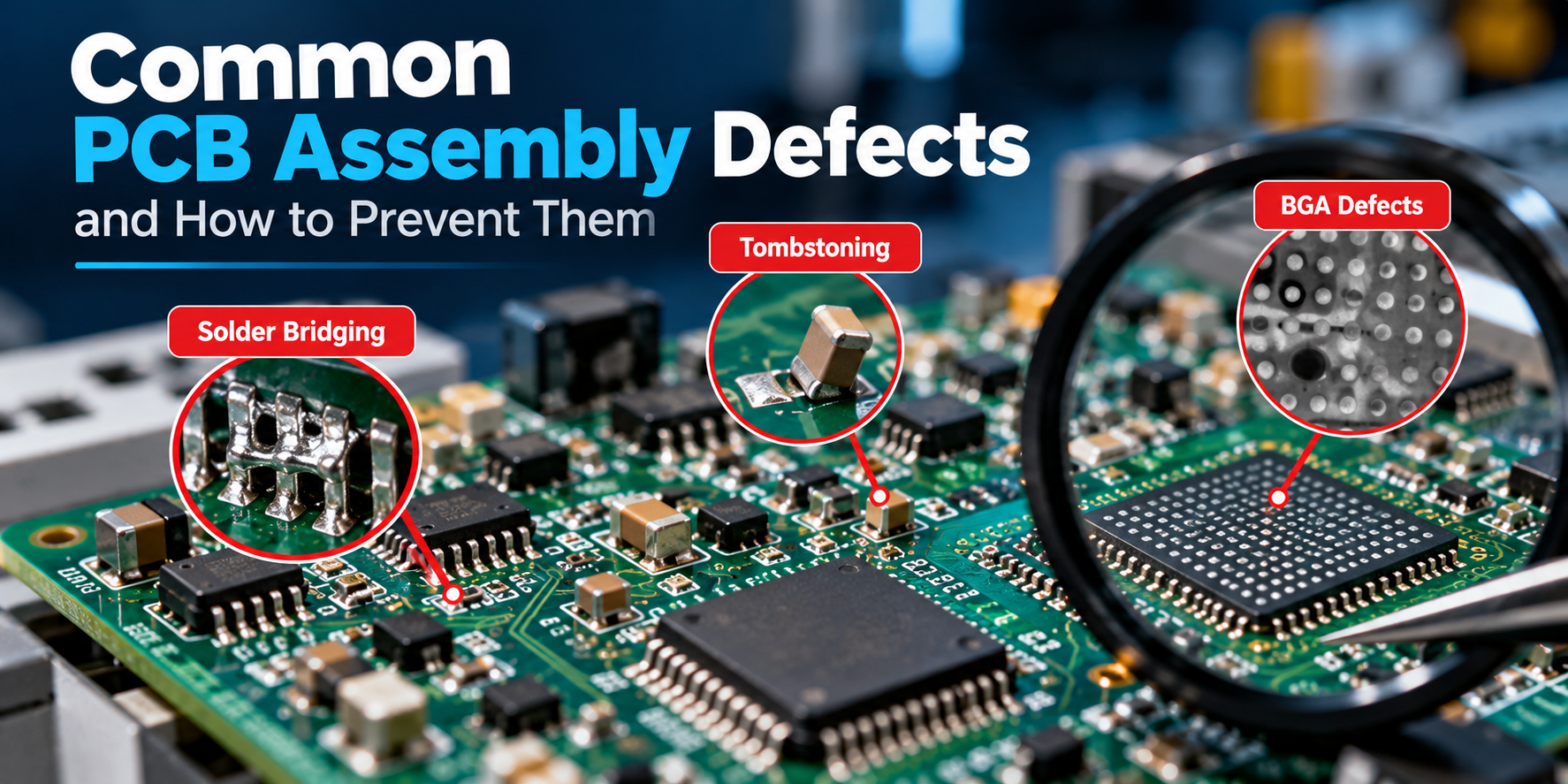
Imagine a newly assembled circuit board that looks perfect during inspection. Every component is positioned correctly, and the solder joints appear clean. Then the technician connects the power supply. The board fails. After testing, the team discovers a tiny solder bridge connecting two pins. One small defect has caused additional inspection, rework, and production delays.
This is why PCB troubleshooting and defect prevention are essential in electronics manufacturing. PCB assembly defects can occur during solder paste printing, component placement, soldering, and handling. Understanding their causes helps manufacturers reduce failures and improve product reliability. This guide explains common PCB defects, detection methods, troubleshooting steps, and practical prevention techniques.
What Are the Most Common PCB Assembly Defects?
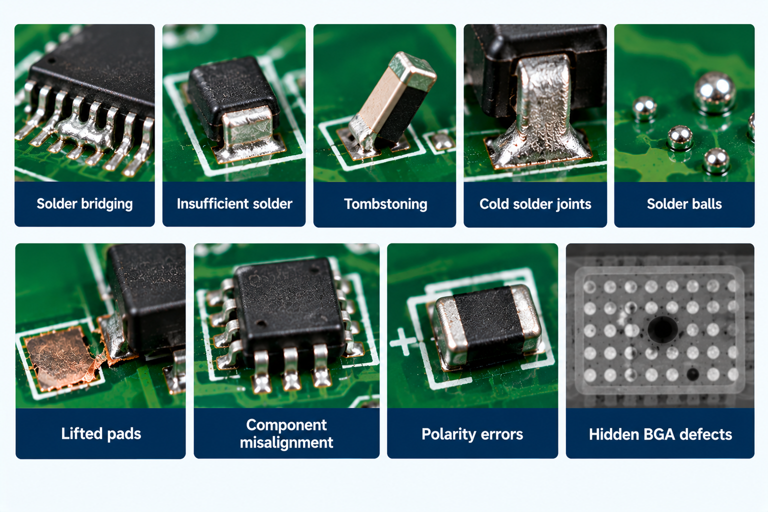
Common PCB assembly defects include solder bridging, insufficient solder, tombstoning, cold joints, lifted pads, component misalignment, polarity errors, and hidden BGA faults.
| PCB Defect | Common Cause | Prevention |
| Solder bridging | Excess solder paste | Optimize stencil design |
| Insufficient solder | Low paste volume | Monitor paste printing |
| Tombstoning | Uneven heating | Balance pad geometry |
| Cold solder joints | Poor solder wetting | Control soldering temperatures |
| Solder balls | Paste or reflow issues | Optimize reflow conditions |
| Lifted pads | Excessive heat | Control rework temperatures |
| Component misalignment | Placement errors | Calibrate assembly equipment |
| Polarity errors | Incorrect orientation | Verify component markings |
| Hidden BGA defects | Voids or open joints | Use X-ray inspection |
Solder Bridging
Solder bridging occurs when excess solder connects adjacent component leads or pads, creating an unintended electrical connection.
It can cause short circuits and complete board failure. Manufacturers can prevent it through accurate stencil design, controlled solder paste application, and proper component placement.
Insufficient Solder and Open Joints
Insufficient solder prevents components from forming reliable electrical connections. Common causes include low solder paste volume, contamination, and inadequate solder wetting.
Controlling paste deposition and soldering conditions reduces these failures.
Tombstoning
Tombstoning occurs when a small surface-mounted component lifts from one pad during reflow soldering.
Uneven heating and unbalanced solder forces are common causes. Proper pad design and optimized reflow profiles help prevent it.
Cold Solder Joints
Cold solder joints develop when solder fails to bond correctly with component leads or pads.
These defects can create intermittent electrical problems. Maintaining appropriate soldering temperatures and clean surfaces improves connection quality.
Lifted Pads and Misalignment
Lifted pads occur when copper separates from the PCB surface because of excessive heat or mechanical stress.
Misalignment happens when components move away from their intended positions.
Controlled rework, careful handling, and accurate placement equipment reduce these problems.
Hidden BGA Defects
Ball Grid Array components contain solder connections underneath their packages.
These connections cannot be fully inspected visually. X-ray inspection helps detect hidden voids, bridges, and open joints.
Industry standards such as IPC-A-610 and J-STD-001 provide guidance for assembly acceptance and soldering requirements.
Cusack Electronics provides electronic PCB assembly services for SMT, through-hole, and mixed-technology boards.
How Does PCB Defect Detection Work?
PCB defect detection combines inspection technologies to identify manufacturing problems before finished boards reach customers.
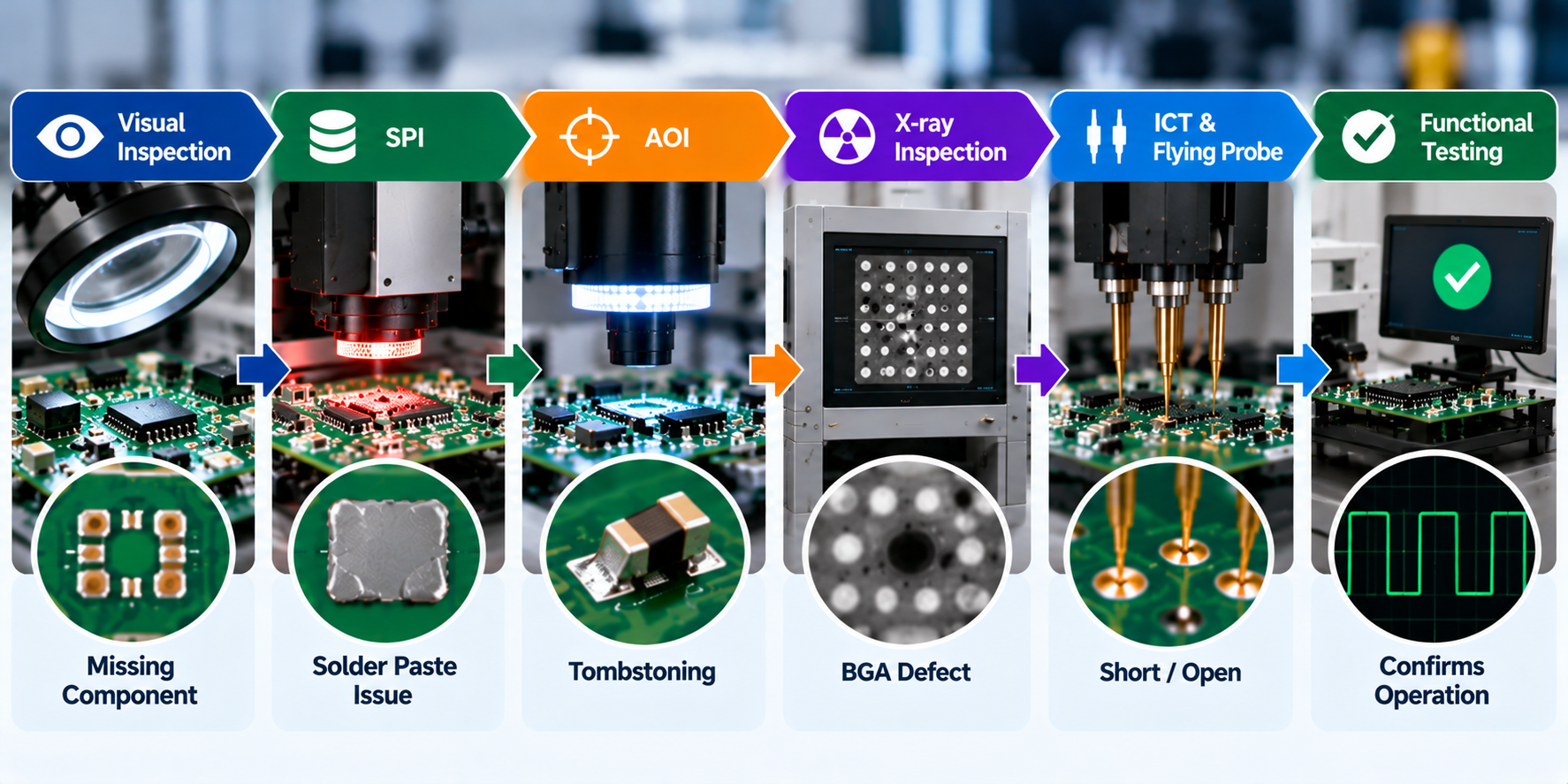
Each method detects different defects.
| Detection Method | Purpose |
| Visual inspection | Identifies visible damage and missing components |
| SPI | Checks solder paste volume and alignment |
| AOI | Detects placement and visible soldering defects |
| X-ray inspection | Reveals hidden BGA solder defects |
| ICT and flying probe | Identifies electrical shorts and open circuits |
| Functional testing | Confirms circuit board operation |
Visual inspection helps identify obvious problems, while solder paste inspection (SPI) checks printing quality before component placement.
Automated Optical Inspection (AOI) detects visible assembly errors, including missing components and solder bridging.
X-ray inspection evaluates connections hidden beneath packages. Electrical and functional testing verify whether assembled circuits operate correctly.
Combining inspection methods improves defect coverage because no single technology identifies every failure.
Learn more in our PCB testing methods guide.
How Do You Troubleshoot PCB Circuits Step by Step?
Following a systematic process makes troubleshooting PCB circuits more efficient and helps identify the actual cause of failure.
- Inspect visually: Look for damaged traces, solder bridges, cracked joints, and incorrect component placement.
- Check power: Measure supply voltages and verify power distribution.
- Test continuity: With power disconnected, check relevant connections for unexpected shorts or open circuits.
- Compare boards: Compare the defective PCB with a known working board.
- Examine signals: Use an oscilloscope to evaluate clock, reset, and communication signals.
- Investigate intermittent faults: Perform appropriate controlled temperature or stress testing.
- Document findings: Record the defect location, root cause, and corrective action.
The final step is particularly important.
If the same soldering problem repeatedly appears around one component, the underlying issue may involve stencil design, component placement, or the soldering process.
Correcting that cause is more effective than repeatedly repairing individual boards.
Why Do PCB Design Reviews Reduce Manufacturing Defects?
Many manufacturing failures begin with problems in the original PCB design.
Poor pad spacing, unsuitable component placement, and missing test points can increase assembly errors.
Early design reviews focus on three areas.
Design for Manufacturability (DFM): Evaluates whether the board can be manufactured consistently.
Design for Assembly (DFA): Improves component placement, accessibility, and assembly efficiency.
Design for Testability (DFT): Ensures that critical electrical connections can be inspected and tested.
These reviews are particularly valuable for high-reliability applications, including defense electronics, where documentation, traceability, and product reliability are important.
Cusack Electronics incorporates engineering reviews into its manufacturing process to identify potential production challenges.
What Happens When PCB Assembly and Box Build Are Split?
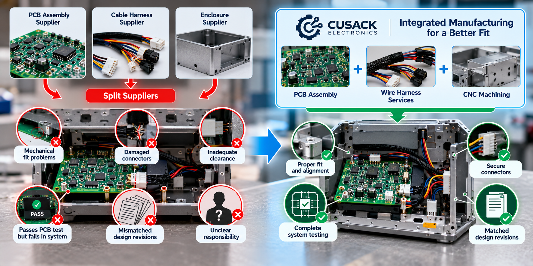
PCB assembly and box build split problems can occur when different suppliers manufacture circuit boards, cable harnesses, and enclosures independently.
Common challenges include mechanical fit problems, damaged connectors, incomplete system testing, unclear responsibility, and mismatched design revisions.
For example, a PCB may pass electrical testing but fail after installation inside an enclosure because of connector stress or inadequate clearance.
An integrated manufacturing approach improves coordination between electronic and mechanical assembly.
Cusack Electronics offers wire harness services and CNC machining alongside PCB assembly.
These capabilities support coordinated manufacturing and help reduce avoidable integration problems.
Frequently Asked Questions
What is the most common PCB assembly defect?
Solder-related defects, including solder bridging, insufficient solder, and open joints, are common assembly problems. Their frequency depends on the manufacturing process.
How can you identify a defective PCB?
Visual inspection, multimeter testing, AOI, X-ray inspection, and functional testing help identify different types of PCB defects.
Can a PCB pass functional testing and still have defects?
Yes. Some marginal solder joints may pass initial testing but fail later under heat, vibration, or mechanical stress.
How can manufacturers prevent PCB assembly defects?
Manufacturers can reduce defects through design reviews, accurate component placement, controlled soldering processes, and layered inspection.
Build Reliable PCBs With Cusack Electronics
PCB assembly defects can cause product failures, costly rework, and manufacturing delays.
Preventing these issues requires careful design, controlled production processes, effective inspection, and systematic PCB troubleshooting.
At Cusack Electronics, we support OEMs and product developers with PCB assembly, engineering, and manufacturing services in Holland, Michigan.
Whether you’re developing a prototype or preparing for production, identifying potential defects early helps improve manufacturing reliability.
Ready to discuss your next PCB project?
Request a Quote to discuss your PCB design and assembly requirements.