
TL;DR: BGA assembly mounts a ball grid array package onto a board by printing solder paste, placing the part, and reflowing so its grid of solder balls melts into joints underneath the body. Every one of those joints is hidden, so X-ray replaces visual inspection and voids become the number people argue about. Design decides most of the outcome: pad size, via strategy, and stencil apertures are set long before the oven runs.
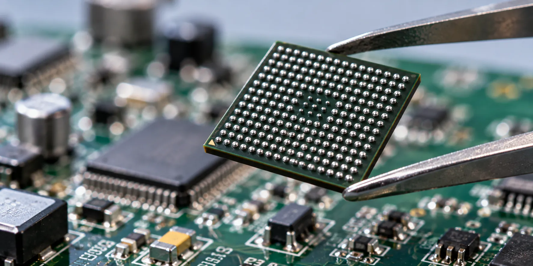
Every other part on a board can be checked by looking at it. A ball grid array cannot, and that single fact drives everything about how these packages get assembled, inspected, and repaired.
So here is my flat opinion, and it is the opposite of what a contract manufacturer is supposed to say. Most BGA failures I see are not soldering failures. They are design failures that only became visible at reflow, and no amount of process tuning rescues a footprint that was wrong before the stencil was cut.
That is why the design section below sits ahead of the rework section, even though rework is what people search for when something has already gone wrong.
What Is a Ball Grid Array?
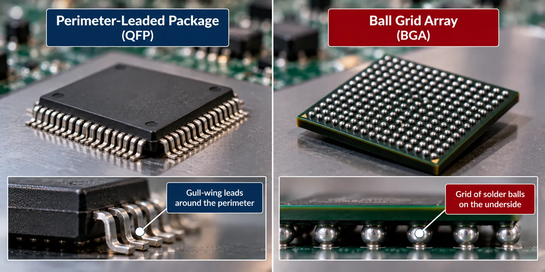
A ball grid array (BGA) is a surface-mount package that carries its connections as a grid of solder balls on the underside of the body, rather than as leads around the edge. Those balls land on a matching grid of pads on the printed circuit board.
Think of the difference between a chair with four legs at the corners and a bed of nails. Perimeter packages get their connections from the edges only, so adding pins means making the package bigger or the pitch finer. A BGA uses the whole bottom face, so the count grows with area.
Wikipedia describes the package as descending from the pin grid array, replacing rigid pins with solder balls attached to pads on the package bottom.
Ball grid array assembly is a branch of surface-mount technology (SMT), not a separate discipline. The same stencil printer, the same placement machine, and the same reflow oven do the work.
Why Designers Choose BGAs
The pin count is the obvious reason. The electrical and thermal behaviour is the better one.
- Shorter connections: a ball sits directly under the die area rather than running out to an edge lead, which cuts inductance and helps at high speed.
- Better heat path: the grid conducts heat down into the board instead of out through thin legs.
- No bent leads: there is nothing to damage in handling, and nothing to coplanarity-check on a reel.
- Less bridging risk at the package: balls are spaced on a grid rather than crowded along an edge.
The trade is simple and permanent. You gain density and lose the ability to see, probe, or touch up a joint after the fact.
What Are the Types of BGA Packages?
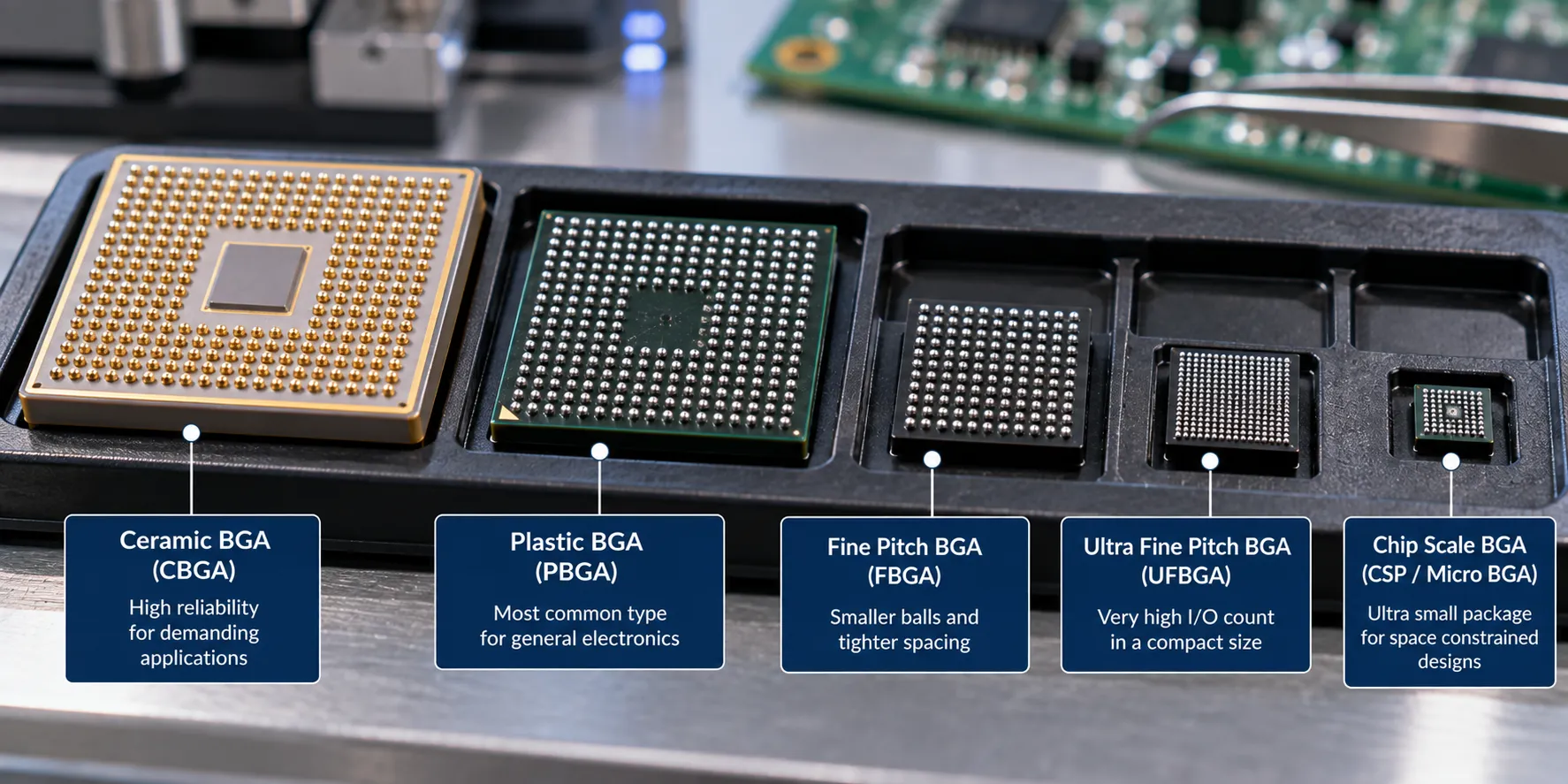
BGA packages are grouped by what the substrate is made of and how fine the ball pitch is, and those two things decide how hard the part is to assemble.
| Type | What it is | Typical pitch | Where it shows up |
|---|---|---|---|
| PBGA | Plastic substrate, the common workhorse | Around 1.0 to 1.27 mm | General-purpose logic |
| CBGA | Ceramic substrate, better thermal match | Around 1.27 mm | High reliability and military |
| FCBGA | Flip-chip die attach, lowest inductance | Around 0.8 to 1.27 mm | Processors and high speed |
| TBGA | Flexible tape substrate, very thin | Around 0.5 to 0.8 mm | Slim mobile devices |
| Micro BGA | Chip-scale, close to die size | Around 0.4 to 0.65 mm | Wearables and compact hardware |
| Thermally enhanced | Integrated heat spreader | Around 1.0 to 1.27 mm | Parts that run hot |
Pitch is the number that matters to whoever assembles it. Anything at 0.5 mm or below changes your via strategy, your stencil, and often your board cost.
A related package worth knowing: an LGA has the same grid of pads but no balls on it, so the solder comes entirely from your paste. That makes paste volume far more critical than on a BGA, where the ball supplies most of the metal.
How Does the BGA Assembly Process Work?
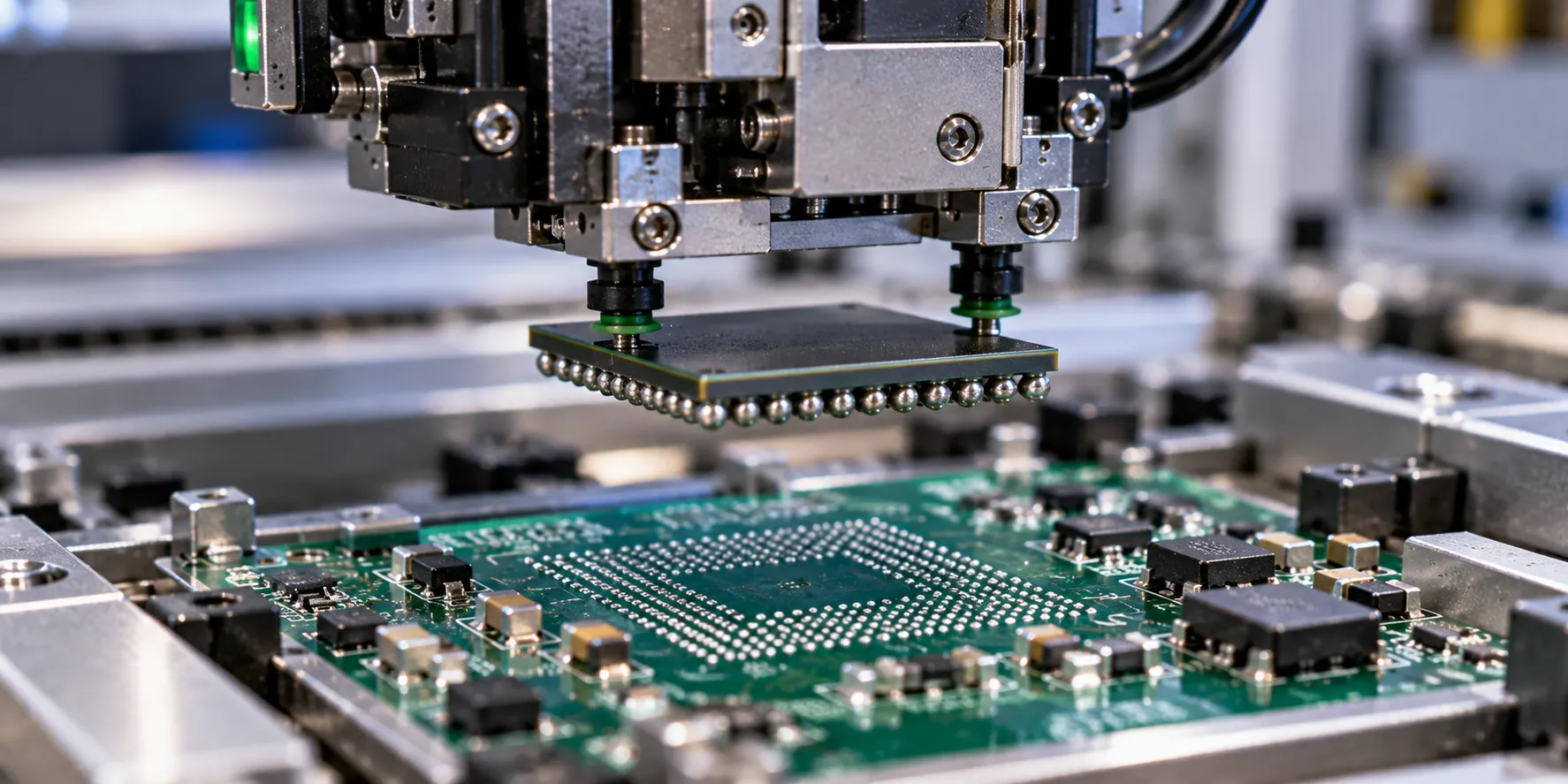
The BGA soldering process uses the same line as every other surface-mount part: print solder paste, place the component, run it through reflow. BGA PCB assembly is not a separate process, just a tighter one, and what changes is the tolerance at every step.
Stencil and Paste
Stencil apertures for BGA pads are usually round, matching the round pad, and slightly smaller than the pad itself.
The reason is counter-intuitive. The ball already contains most of the solder the joint needs, so the paste is there mainly to supply flux and hold the part. Too much paste and you push metal sideways into a bridge.
That is the opposite of an LGA or a fine-pitch passive, where the paste is the whole joint.
Placement and Self-Centring
A pick-and-place machine sets the package onto the paste using its ball pattern, not its body edges, as the alignment reference.
Placement accuracy matters less than people expect, because of what happens next. When the balls melt, surface tension pulls the package into alignment on its own, which is why a part placed slightly off can still come out square.
That self-centring has a limit, and it is worth treating as a working rule rather than a specification. Once a ball sits mostly off its pad, surface tension has nothing to pull against and the part will not recover.
On a fine-pitch package that margin is small, which is why placement still gets checked rather than trusted.
Reflow
The reflow oven melts the ball and the paste together into one joint, and the profile has less margin than on a simple board.
A large BGA is a big thermal mass sitting next to small passives, so the temperature difference across the board is the thing to control. The joints under the middle of a big package are the last to reach liquidus.
Profile from the paste datasheet and the package rating, verified with thermocouples. I have covered how to build that curve properly in my guide to reflow soldering and where this step sits in the wider line in the SMT assembly process.
How Do You Design a Board for BGAs?
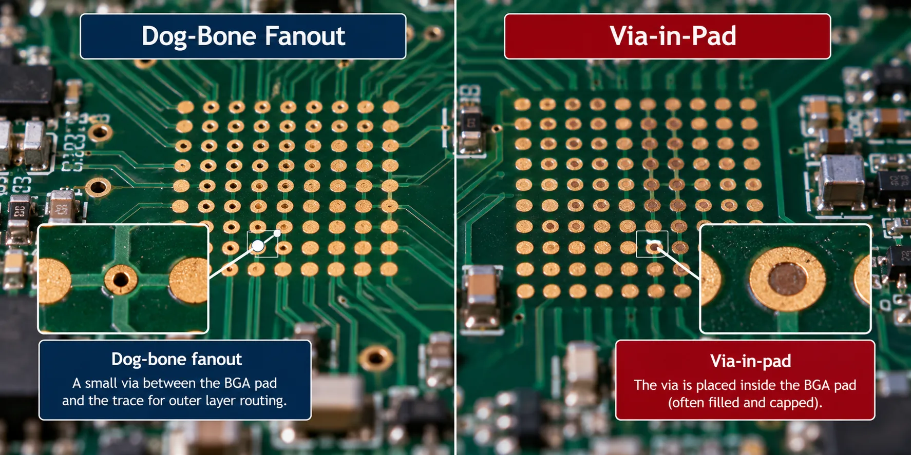
Get the footprint right and the assembly is unremarkable. Get it wrong and no process adjustment saves it.
- Pad type: non-solder-mask-defined pads are generally preferred, because the solder wets the full copper pad rather than being constrained by mask.
- Fanout strategy: at coarser pitches you can run a short trace from the pad to a via, the dog-bone pattern. Below about 0.5 mm pitch that space disappears and you need via-in-pad.
- Via-in-pad must be filled and capped: an open via under a pad wicks solder away and starves the joint. Filled, plated-over vias solve it and cost more.
- Keep the thermal environment even: a ball tied straight into a large plane heats slower than its neighbours, so thermal relief matters here as much as anywhere.
- Leave room for rework: a BGA crowded by tall parts cannot be reached by a rework nozzle without cooking its neighbours.
Once via-in-pad becomes unavoidable, the board itself is built differently, with laser-drilled microvias instead of mechanically drilled holes. That shift is covered in my guide to HDI PCB.
The governing document is worth naming properly, because almost nobody cites the current one.
The current one is IPC-7095E, Design and Assembly Process Guidance for Ball Grid Arrays.
It was published in August 2024, superseding IPC-7095D with Amendment 1, which dated from 2019.
The title changed with that revision, from “Implementation” in every edition since the A revision to “Guidance” in E. If a supplier quotes you IPC-7095 without a letter, ask which one they mean.
This is the stage where a design for manufacturability review earns its fee and where PCB layout design choices become expensive to reverse.
How Do You Inspect a Joint You Cannot See?
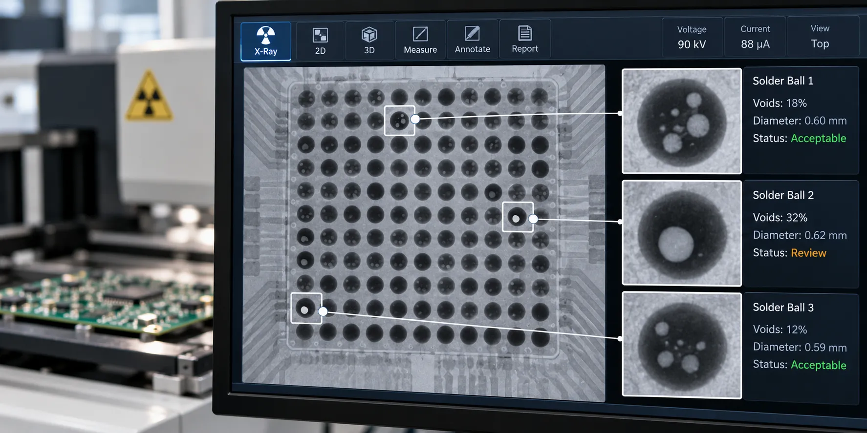
BGA inspection is done by X-ray, because the joints sit underneath the package body where no camera has an angle on them.
An X-ray looks down through the package and shows each ball as a shape. A clean joint reads as an even disc. A bridge shows as two balls merged. A void shows as a lighter patch inside the ball, because there is less metal for the beam to pass through.
Automated optical inspection still runs on these boards, but only to confirm the package is present, right way round, and not skewed. It cannot say anything about the joints themselves.
That is the one place this work departs from ordinary surface-mount technology practice, where a camera settles most questions.
X-ray sits alongside the other checks rather than replacing them, and I have compared the full set in my guide to PCB testing methods.
What Void Level Is Acceptable?
Voids are gas pockets trapped inside a solder ball, and the commonly cited ceiling is around 25 percent of the ball’s area.
The measurement is specific, and getting it wrong is how arguments start. Void percentage is calculated per individual ball, as the total void area inside that ball divided by the ball’s own projected area in the X-ray image, not the copper pad area.
One correction worth making, because plenty of articles state the opposite. The tightening between IPC Class 2 and Class 3 is generally in inspection coverage and surrounding workmanship criteria, not in a different numeric void percentage.
Check the figure that applies to your build against the acceptance standard your contract names, with IPC-7095E for the measurement methodology behind it. A number quoted without its standard and revision is not a specification.
What Goes Wrong in BGA Assembly?
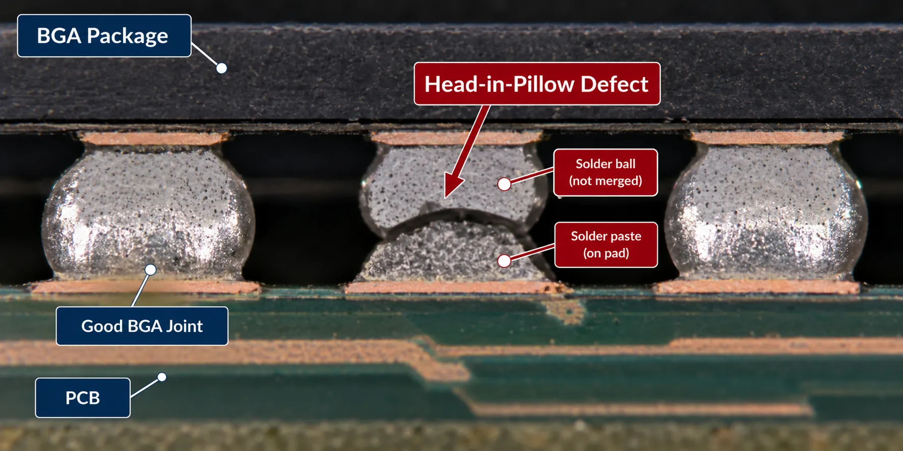
BGA defects fall into two groups: the ones X-ray finds easily, and the one that hides from it.
| Defect | What it is | Usual cause |
|---|---|---|
| Bridging | Two balls merged into one joint | Too much paste, or package skewed at placement |
| Voiding | Gas trapped inside a ball | Flux outgassing, profile, or via-in-pad not capped |
| Open joint | Ball never touched the pad | Board or package warping at peak temperature |
| Head-in-pillow | Ball and paste both melted but never merged | Warping, or flux spent before liquidus |
| Popcorning | Package cracked internally by trapped moisture | Floor life exceeded, no bake before reflow |
| Pad cratering | Laminate fractured under the pad | Mechanical stress, often after rework |
Head-in-pillow is the difficult one. The ball sits against the pad looking almost right, so a 2D X-ray can pass it, and the board can even work on the bench before failing in the field.
Popcorning is the avoidable one. Plastic packages absorb moisture and need baking once their floor life runs out, which is classified under IPC/JEDEC J-STD-020F, reissued in 2022.
When a joint has to be understood rather than just passed or failed, there is a destructive option: dye and pry. You flood the assembly with penetrating dye, break the package off, and read which joints the dye reached. It sacrifices the board and answers the question properly.
How Does BGA Rework Work?

BGA rework removes a fitted package, cleans the site, and fits a replacement, all using localised heat so the rest of the printed circuit board survives.
- Remove. The board is preheated from below while a top heater runs a profile over the package alone. Once the balls reach liquidus, a vacuum nozzle lifts the part straight off.
- Redress the site. The pads are left with uneven, oxidised solder. Flux and desoldering braid wipe them flat.
- Reball, or replace. Fitting fresh balls to the removed package through a stencil is reballing. Fitting a new package instead skips it.
- Align. A split-optics camera overlays the package’s ball image onto the pad image so the operator can correct X, Y, and rotation.
- Reflow again. The station runs a second profile to form the new joints.
Baking comes first on any moisture-sensitive package. Skipping it is how a rework job cracks a part that was fine before you touched it.
Rework or Reball?
Reballing restores the package. Rework replaces the joint. They get confused because a reball usually happens inside a rework job.
Reball when the package is expensive, obsolete, or unobtainable and the die is known good. Fit a new part whenever you can get one, because it is faster and carries less risk.
Here is the part a contract manufacturer is not meant to say: on a cheap board with a cheap package, rework is often the wrong call. Every cycle puts the laminate through another peak, and pad cratering after a second or third rework is common. Price the replacement board before you price the repair.
Frequently Asked Questions
Can you solder a BGA by hand?
Not properly. There is no way to reach the joints with an iron, and heating from above through the package body gives you no control over what the balls are doing. Hot air can reflow a BGA in a pinch, but without bottom-side preheat and a measured profile the result is a lottery.
How do you know a BGA is soldered correctly without seeing it?
X-ray for the joints, electrical test for the function, and boundary scan where the device supports it. Boundary scan is useful because it exercises the connections through the chip itself, catching opens that a 2D X-ray image can pass.
What is the smallest BGA pitch you can assemble?
It depends more on the board than the placement machine. Pitches around 0.4 mm are routine for shops set up for them, but below roughly 0.5 mm you need via-in-pad, filled and capped, and a stencil to match. The limiting factor is usually fabrication cost.
Why do BGA joints crack after the board has been working fine?
Thermal cycling. The package and the board expand at different rates, and each heating cycle works the joint slightly. Ceramic packages on standard laminate are the classic case, which is why underfill is used on parts that see wide temperature swings.
Does every BGA board need X-ray inspection?
Not every board, but every new design and every process change. Once a design is running with a stable profile and clean results, sampling is reasonable. First articles and any build after a change should be X-rayed fully.
Can a BGA be reworked more than once?
Sometimes, but treat each cycle as damage. The pads and laminate take a full thermal excursion every time, and pad cratering gets more likely with each one. Two is a reasonable practical ceiling on most standard boards.