THE 30-SECOND VERSION
A solder paste stencil is a thin metal foil with an opening cut over every pad, used to print the exact volume of paste each joint needs. Two numbers govern it: area ratio, which decides whether paste releases from the hole, and thickness, which sets how much lands on the pad. The widely quoted minimum area ratio of 0.66 is a property of ordinary laser-cut stainless steel, not a law, and better stencil technology beats it.
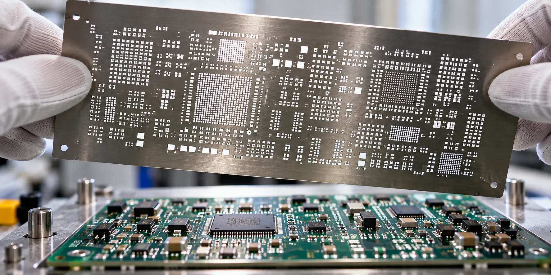
The stencil is the cheapest item on an SMT line and the one that decides most of your defect rate. That imbalance is why it is worth half an hour of attention before you order one.
Here is my flat opinion. Most stencil problems are ordered in, not printed in. By the time a board is on the printer, the thickness is fixed, the apertures are cut, and your remaining options are squeegee pressure and hope.
So this covers what to decide before the file goes to the stencil house, including one number almost everyone repeats without the caveat attached to it.
What Is a Solder Paste Stencil?
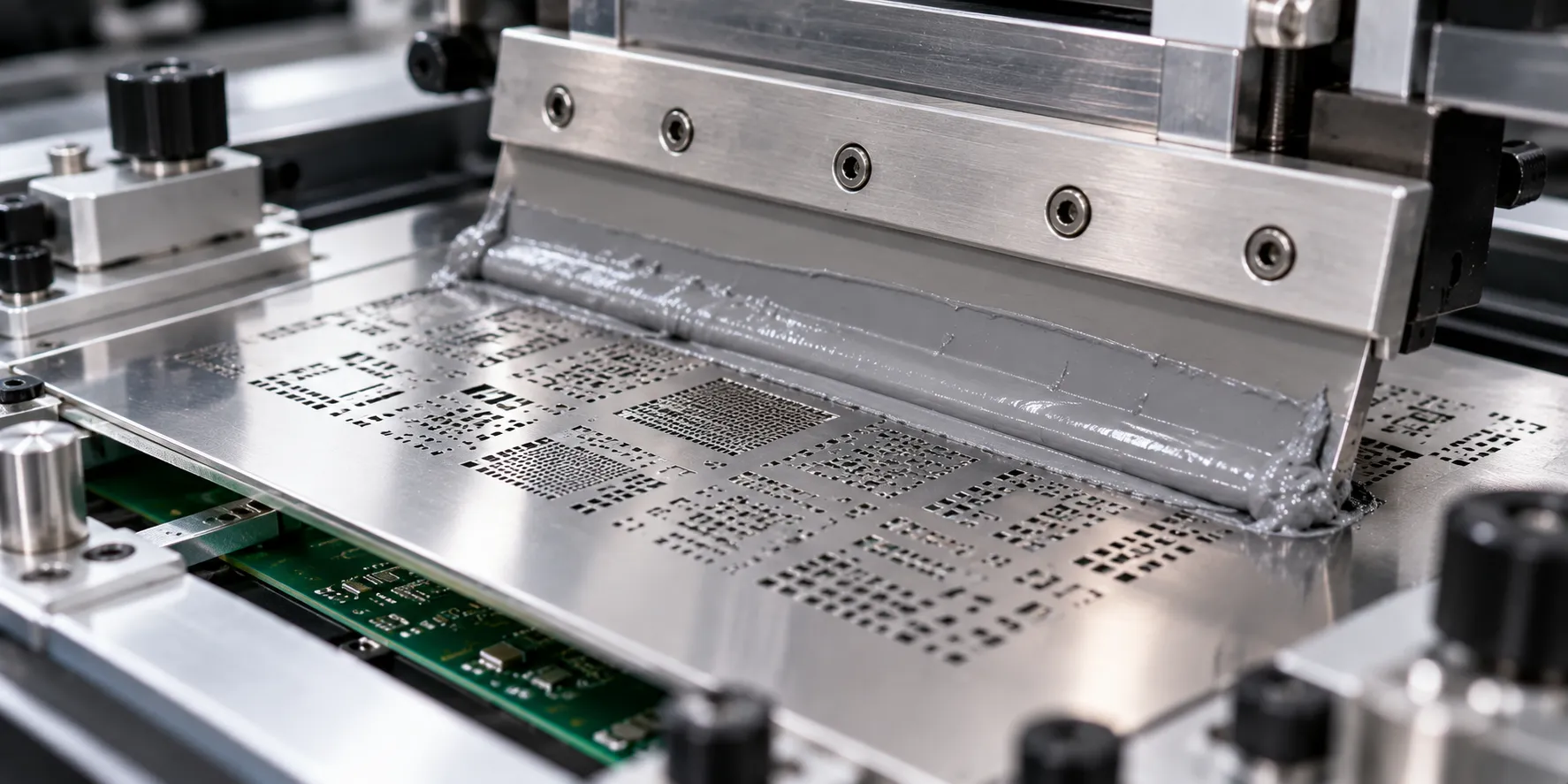
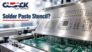
A solder paste stencil is a thin metal foil, usually stainless steel, with an aperture cut through it above every pad that needs paste.
Think of it as a stencil in the ordinary sense, the kind used to spray a letter onto a wall. The foil blocks paste everywhere except the holes, so the pattern that lands on the board is exactly the pattern you cut.
In use it sits in a stencil printer, clamped over the board and aligned to fiducial marks etched on the board surface. A squeegee drags paste across the foil, fills the apertures, and the stencil lifts away.
What stays behind on each pad is the deposit that becomes a solder joint in reflow soldering. Get the volume wrong and no amount of oven tuning recovers it, which is why solder paste inspection sits immediately after printing on most lines.
Printing is the first station on the line, and where it sits relative to placement, reflow and inspection is covered in my guide to the SMT assembly process.
What Are Area Ratio and Aspect Ratio?
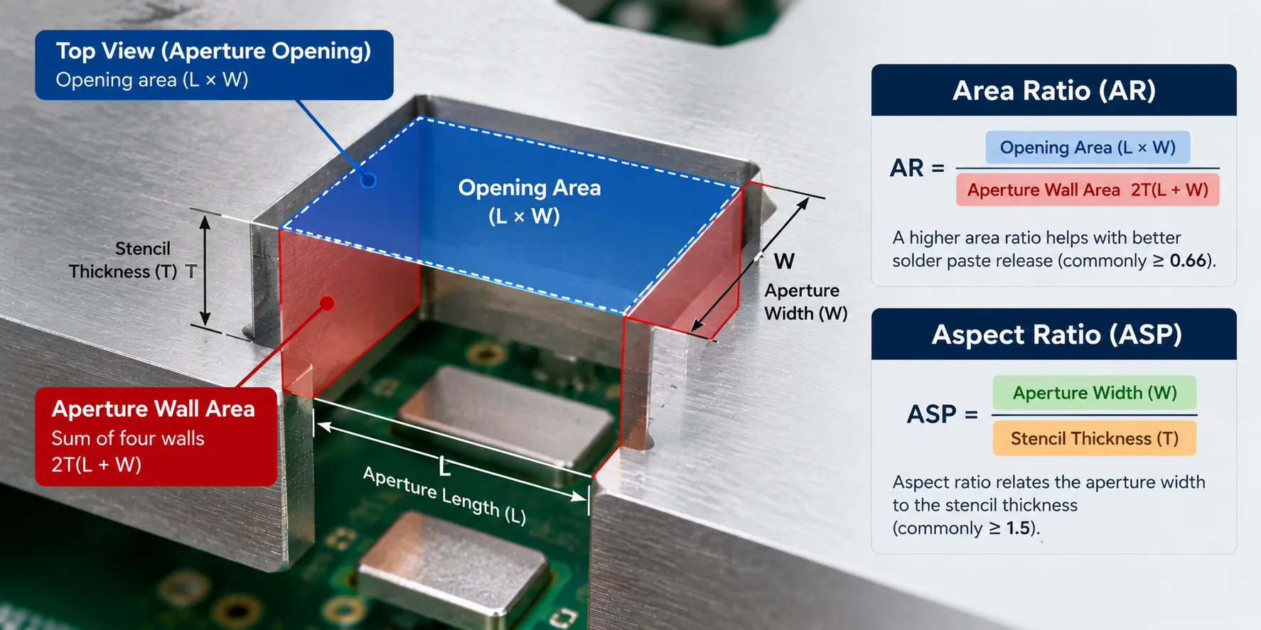
Stencil aperture ratio describes whether paste will come out of the hole. Two versions exist, and the one that matters most is area ratio.
Area ratio is the area of the aperture opening divided by the area of its walls. For a rectangular aperture:
Area Ratio = (L x W) / (2 x (L + W) x T)
where L and W are aperture length and width, and T is stencil thickness.
Aspect ratio is simpler: aperture width divided by foil thickness. It is the older measure and still useful, but it ignores aperture shape, so it misleads on long thin openings.
Here is the physics in plain terms. As the stencil lifts, paste has to choose between sticking to the pad below and sticking to the aperture walls around it.
A wide, shallow hole gives paste more pad to grip than wall, so it releases. A narrow, deep one does the opposite and leaves a plug behind.
Is 0.66 Really the Minimum?
It is the conventional floor, and it is a property of the stencil, not of physics. That distinction is worth understanding before you redesign a board around it.
The figure comes from ordinary laser-cut stainless steel, where aperture walls are comparatively rough and paste clings to them. Rougher walls, worse release, higher minimum ratio.
Rachel Miller Short and William E. Coleman of Photo Stencil, with Joseph Perault of Parmi, tested twelve stencils against a published criterion.
That criterion was more than 80 percent paste transfer with under 10 percent volume standard deviation.
Electroformed foil with a nano coating met that criterion down to area ratios of 0.33 to 0.39, roughly half the conventional floor. The electroformed stencils had the smoothest walls in the test; laser-cut stainless the roughest.
That paper carries no publication date and cites 2009 conference work, so treat the exact figures as a decade-old snapshot rather than today’s capability. Coatings have moved on since, which only strengthens the direction of the finding.
The practical takeaway: if your area ratio lands between 0.5 and 0.66, that is a conversation with your stencil supplier about foil and coating, not an automatic board respin.
How Thick Should a Stencil Be?
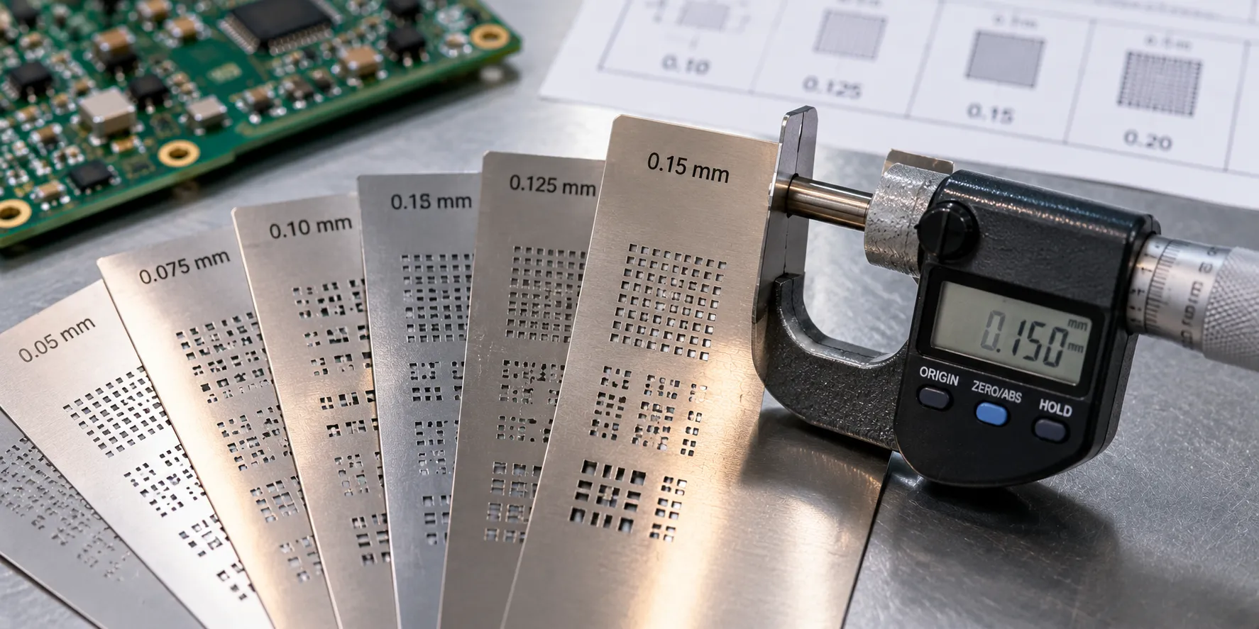
Stencil thickness is set by the finest-pitch part on the board, not by the average part. Most production foils sit between 0.10 and 0.20 mm, commonly quoted as 4 to 8 thou.
Thickness works against you in both directions. Thicker foil deposits more paste, which large connectors and shielding cans want, but it drives area ratio down on the small apertures and starves them.
- 0.10 to 0.13 mm: ultra-fine pitch, 0201 passives, fine-pitch QFN and small BGA.
- 0.13 to 0.15 mm: the common general-purpose range for mixed surface-mount boards.
- 0.15 to 0.20 mm: boards dominated by larger passives, connectors, and through-hole parts filled by paste.
Run the area ratio sum on your smallest aperture before committing. If it fails, the choice is a thinner foil, a different foil technology, or a step stencil.
What Are the Core Stencil Aperture Design Rules?
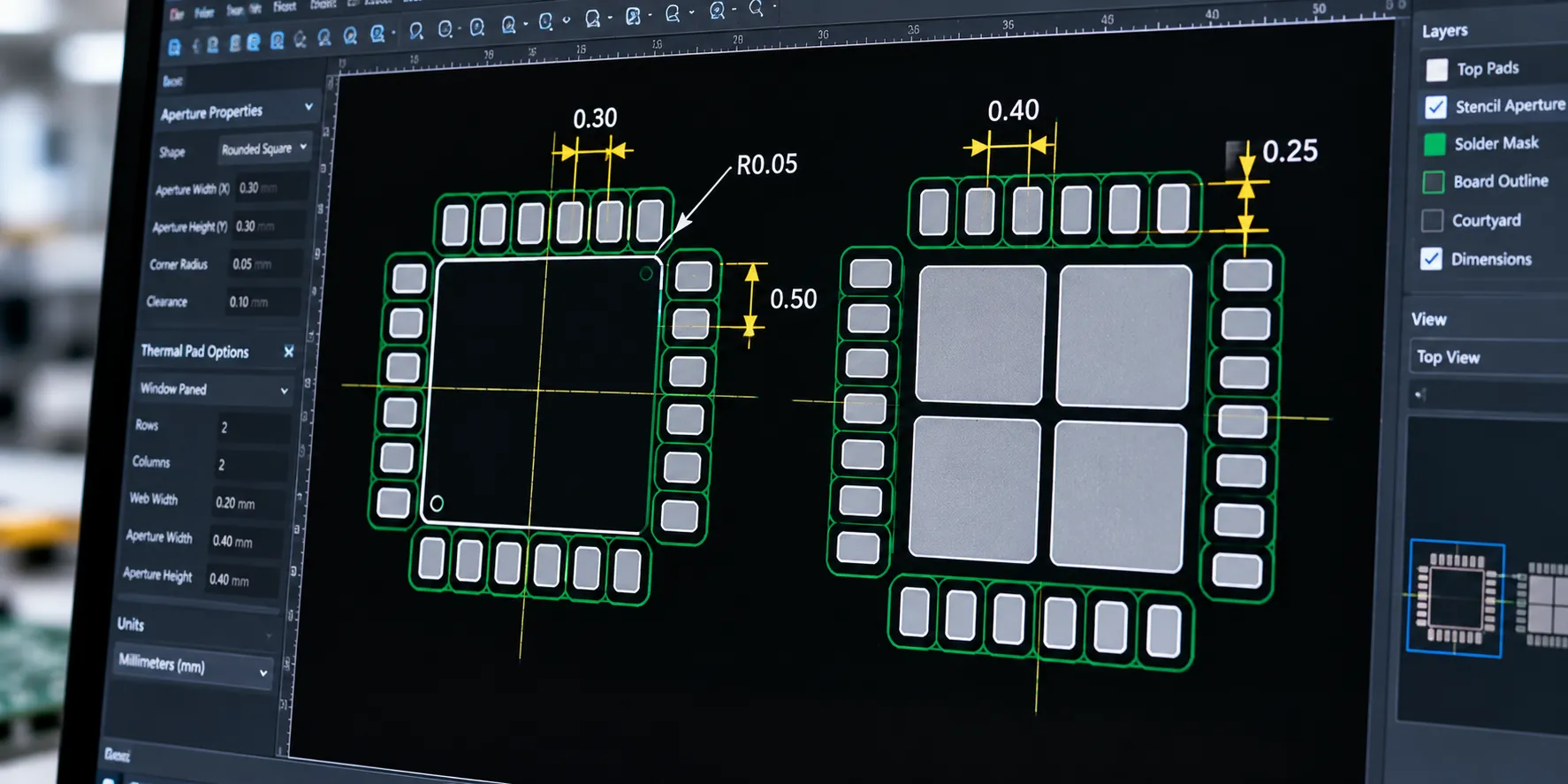
Stencil aperture design starts from the pad, then departs from it deliberately wherever the pad shape would cause a defect.
- Reduce apertures on fine-pitch parts. Printing 100 percent of pad area on a fine-pitch lead bridges it. Reductions in the region of 10 to 20 percent are common, applied per part type rather than globally.
- Prefer square or rectangular apertures with rounded corners over circles on small pads. Squares carry more open area for the same wall perimeter, so they release better.
- Windowpane large thermal pads. A single big opening floats the part on a dome of solder. A grid of smaller openings covering roughly half to three quarters of the pad area gives the heat path without the lift.
- Keep apertures off board features. An aperture overlapping a via or a mask edge will not seal, and paste escapes underneath.
- Match the fiducial set. The stencil needs its own fiducials to align to the board’s, and they have to be cut, not printed.
The thermal pad rule is where I see the most expensive mistakes, because the failure looks like a reflow soldering problem when it started at the printer.
I have covered that case in my guide to the QFN package.
The BGA case runs the other way, because the ball supplies most of the solder, which I have explained in my guide to BGA assembly.
The governing document is IPC-7525, Stencil Design Guidelines.
The current revision is IPC-7525C, published November 2021 to replace IPC-7525B from 2011.
Its table of contents is public even though the standard is not, and it reads as a useful checklist of what a stencil decision covers.
When Do You Need a Step Stencil?
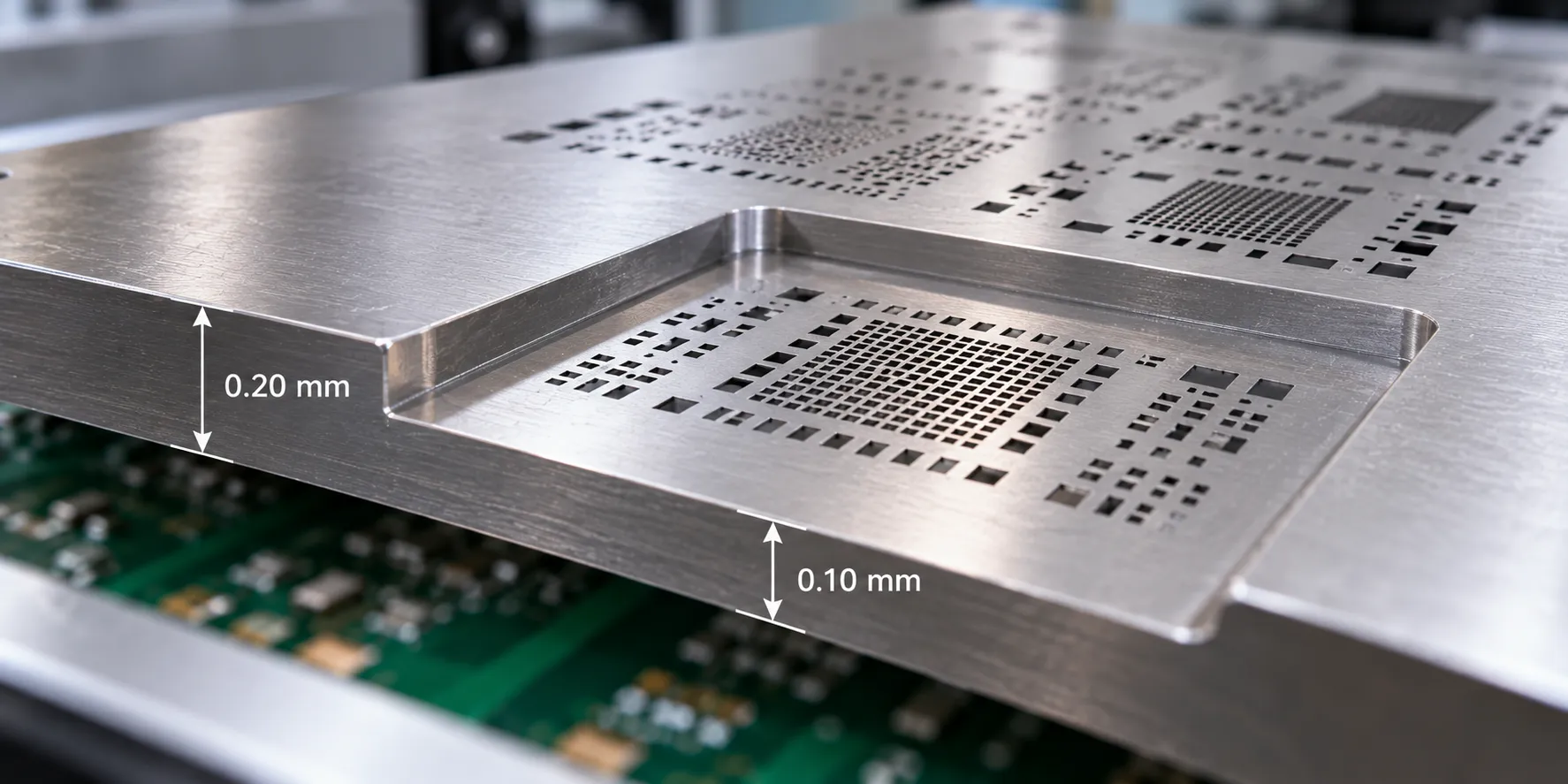
A step stencil has areas of different thickness in one foil, so parts with incompatible paste needs can share a board.
Picture a board carrying 0201 chip resistors beside a heavy power connector. The resistors need a thin foil to release cleanly; the connector needs bulk paste. One uniform thickness cannot serve both.
- Step-down thins the foil locally over fine-pitch areas, which is the common case.
- Step-up thickens it locally where extra volume is wanted, often for connectors or shields.
- Relief etch removes material from the squeegee side rather than cutting a full step, a gentler variant IPC-7525 treats separately.
Steps are not free. They cost more, they need clearance around the transition so the squeegee does not skip, and a badly placed step smears paste across the boundary.
So treat a step stencil as a fix for a real conflict, not as a default. If moving one connector solves the problem, move the connector.
Laser-Cut, Electroformed, Framed or Frameless?
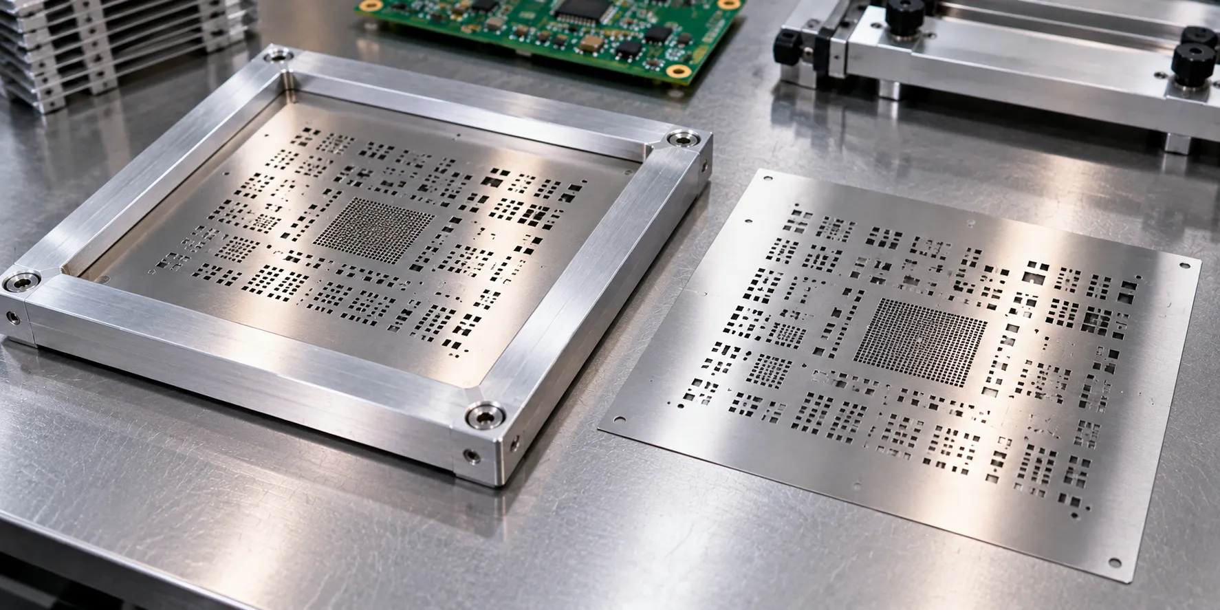
Two separate decisions get confused here. How the foil is made is one question; how it is held is another.
| Laser-cut stainless steel | Electroformed | |
|---|---|---|
| How it is made | Laser cuts apertures in rolled foil | Nickel grown onto a mandrel |
| Aperture walls | Rougher, slightly tapered | Smoothest available |
| Paste release | Good, better with a nano coating | Best, reaches lower area ratios |
| Cost | Lower | Higher |
| Best for | Most production work | Ultra-fine pitch and tight area ratios |
A laser cut stencil is the default and the right answer for the large majority of boards. Electroformed is a targeted fix when the area ratio sum will not close.
Nano coating sits between the two. It is a surface treatment applied to the foil and aperture walls that reduces paste sticking, and it improves release on laser-cut stencils enough to be worth asking about on fine-pitch work.
Then the mounting question. Framed versus frameless stencil comes down to volume and storage, not print quality.
- Framed: the foil is permanently bonded into a tensioned frame. Best for production runs that repeat, fastest to load, bulky to store.
- Frameless: a bare foil that mounts into a reusable tensioning frame. Cheaper, far easier to store, an extra step at changeover.
For a shop running many different boards in short runs, frameless wins on storage alone. For a board that runs every week, framed earns its space.
Frequently Asked Questions
How long does a solder paste stencil last?
There is no fixed cycle count. A stencil is retired when apertures distort, the foil creases, or print quality drifts despite correct settings. IPC-7525C includes an end-of-life section for exactly this reason. Inspect the foil at changeover, and treat a sudden rise in paste inspection rejects as a stencil question, not only a printer question.
What information does a stencil house need to quote?
Gerber data including the paste layer, the board outline, foil thickness, framed or frameless, and any step requirements. The paste layer is the one most often missing. Without it the supplier builds apertures from your copper layer, which means every reduction and every windowpane is their guess rather than your decision.
Can I reuse a stencil from a previous revision?
Only if the paste layer did not change, and that includes pad geometry, not just part positions. A revision that moved one connector by a millimetre makes the old foil scrap. Checking takes a minute; discovering it on the printer costs a build slot.
Does stencil cleaning really matter between prints?
Yes, more than most people expect. Paste builds up on the underside of the foil and starts bridging deposits beneath the apertures. Printers wipe automatically at a set interval, and that interval is a real process parameter worth tuning rather than accepting as shipped. A drift in solder paste inspection results is usually the first sign it is set too long.
Should I use the same aperture reduction on every part?
No, and this is a common shortcut that causes bridging on fine-pitch parts and starved joints on larger ones. Reductions belong per component family, driven by pitch and pad geometry. A single global percentage is the fastest way to make one half of the board worse while fixing the other.