THE 30-SECOND VERSION
An HDI PCB is a high-density interconnect board that uses laser-drilled microvias and fine-line routing to fit more connections into less area than a conventionally drilled board. The technology is what makes fine-pitch parts routable at all. Two things trip people up: the IPC type numbers do not mean what most articles say they mean, and stacking microvias deep costs you reliability in a way the marketing pages rarely mention.

A high-density interconnect PCB is not a premium version of an ordinary board. It is a different way of building one, and the difference starts at the drill.
Here is my flat opinion. Most designs that end up specified as high-density interconnect did not need to be, and a smaller number that desperately needed it were laid out as conventional boards and then failed to route. Neither mistake is expensive to avoid, and both are expensive to discover at the fabrication quote stage.
So this piece covers what the technology actually is, what the IPC types genuinely say, and where the reliability limits sit. That last part is where I found the most interesting number.
What Is an HDI PCB?
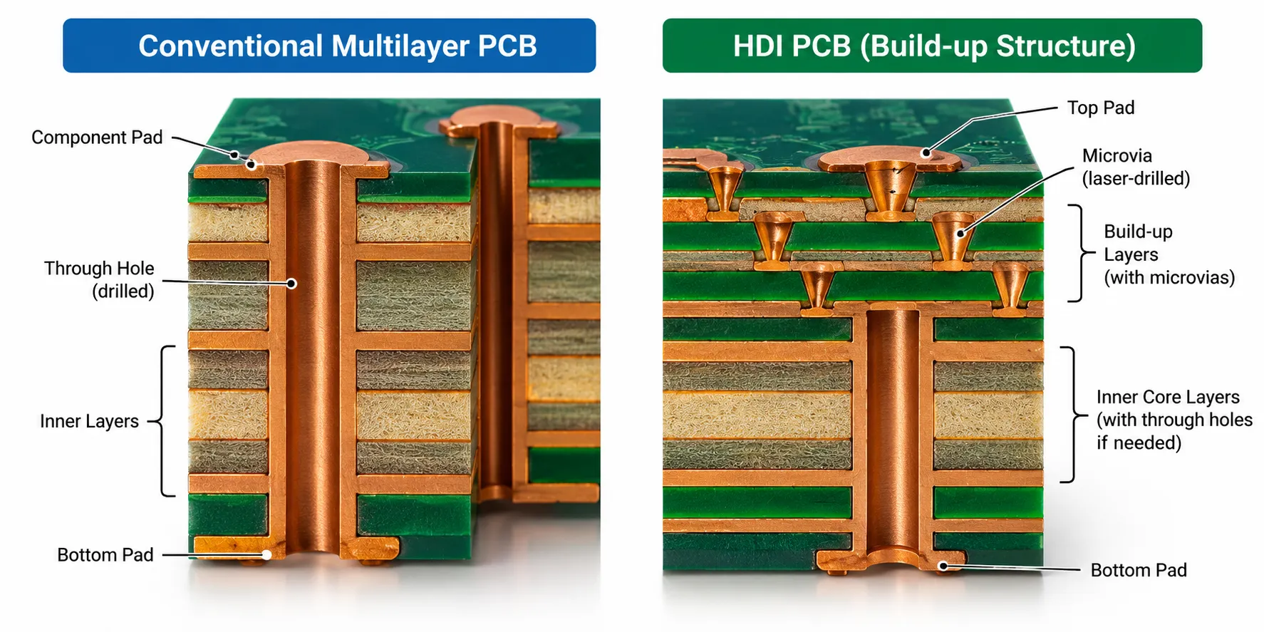
An HDI PCB, short for high-density interconnect printed circuit board, is a multilayer circuit board that achieves higher wiring density per unit area than a conventional board by using microvias, finer lines, and thinner dielectric layers. It is a multilayer PCB first and foremost; what changes is how the layers get joined.
Think of it as the difference between a town with only main roads and one that also has alleys. A conventional board connects layers with holes drilled clean through the whole stack, so every connection takes up space on every layer it passes. High-density interconnect adds short local connections that only go where they are needed.
That is the whole idea. Less space wasted on connections you did not want means more space for the ones you did.
What Makes a Board “High Density”?
Density here is measured in what you can fit, not in how many layers you have.
- Microvias instead of mechanically drilled through holes for the outer connections.
- Fine-line circuit routing, with trace widths and spacing well below what standard fabrication holds.
- Thin dielectrics, because a laser cannot drill deep and a shallow via needs a shallow layer to cross.
- Sequential build-up, meaning the board is laminated in several stages rather than pressed once.
- Via-in-pad, letting a connection drop straight down from a component pad instead of routing out to a via first.
The last one is usually what forces the decision. A fine-pitch ball grid array simply has nowhere to put an escape trace, which I have covered from the assembly side in my guide to BGA assembly.
What Is a Microvia?
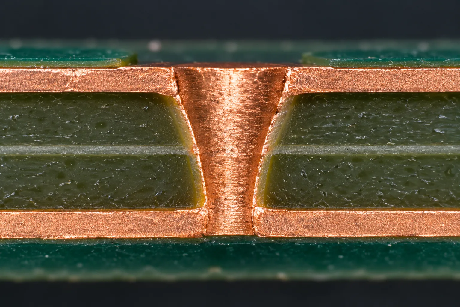
A microvia is a very small hole connecting adjacent layers, formed by laser drilling rather than by a mechanical drill bit.
The definition is dimensional, not descriptive.
Under the IPC definition revised in 2013, a microvia is a hole with a depth-to-diameter aspect ratio of 1:1 or less, with depth not exceeding 0.25 mm.
The earlier criterion was simpler: any hole 0.15 mm or smaller in diameter.
That aspect ratio limit is the physics of the process. A laser ablates a shallow, slightly tapered pit, and it cannot reach far without the hole becoming impossible to plate evenly.
Two related terms get used alongside it constantly. A blind via connects an outer layer to an inner one without passing through the board. A buried via connects inner layers only, with no opening on either surface.
Should Microvias Be Stacked or Staggered?
Stagger them where the layout allows, and this is the part of high-density interconnect design I would push hardest on.
Stacked microvias sit directly on top of each other, one per layer, forming a vertical column. Staggered microvias step sideways at each layer, so no via sits on the one below it.
Stacking is tidier and saves space. It also concentrates thermal expansion stress in a single column, and the failure modes that follow are well documented: interfacial separation, barrel cracks, corner cracks, and cracked pads.
How much does depth matter? Research cited in the microvia literature by Birch found that two-level stacked microvias survived roughly twenty times more thermal cycles than four-level stacks.
That number is worth sitting with before anyone signs off a four-high stack on a product that will see real temperature swings. Stagger if you can, keep stacks shallow if you cannot, and treat a deep stack as a decision that needs justifying.
What Are the HDI PCB Types?
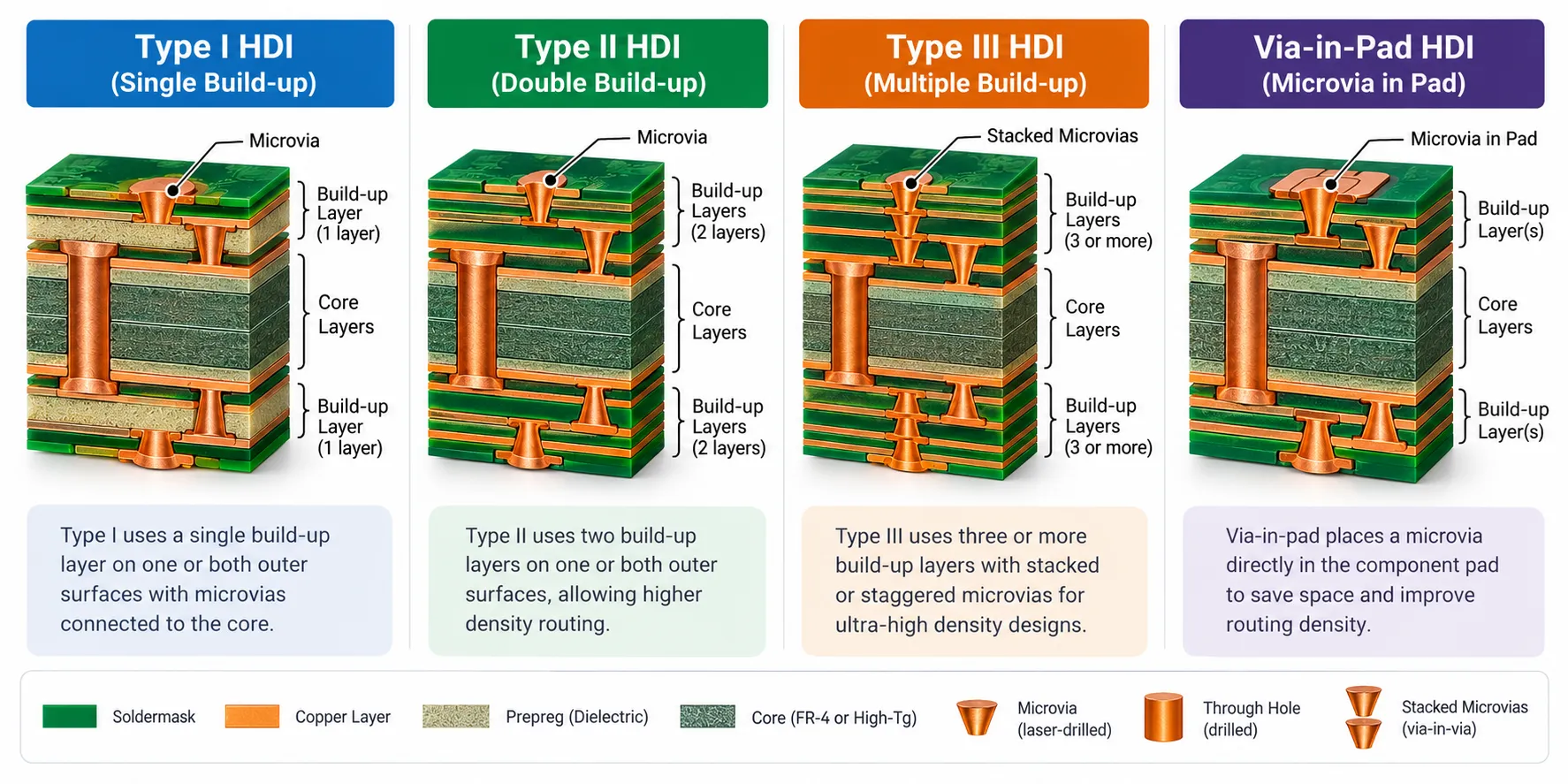
The HDI PCB types come from IPC-2226A, Sectional Design Standard for High Density Interconnect Printed Boards, published in 2017 to supersede the 2003 original.
Read this table carefully, because a lot of published material gets it wrong. In IPC’s notation, C is a core and P is a passive substrate.
| Type | What IPC-2226A specifies |
|---|---|
| Type I | 1 [C] 0 or 1 [C] 1, with through vias connecting the outer layers |
| Type II | 1 [C] 0 or 1 [C] 1, with buried vias in the core, and may have through vias |
| Type III | Two or more build-up layers on at least one side, may have buried and through vias |
| Type IV | At least one build-up layer over a passive substrate with no electrical connection |
| Type V | Coreless constructions using layer pairs |
| Type VI | Alternate constructions |
Here is the correction worth making. The types are distinguished by construction, specifically what sits in the middle and how the vias reach it, not simply by how many build-up layers you count.
Plenty of widely read articles map Type I to “1+N+1”, Type II to “2+N+2” and Type III to “3+N+3”, marching up in step. That is not what the standard says, and Type IV is a passive substrate construction rather than an advanced any-layer one.
If a fabricator quotes a type number, ask them to describe the construction in words as well. It takes one sentence and removes an entire category of misunderstanding.
How Do You Read an HDI Stackup?
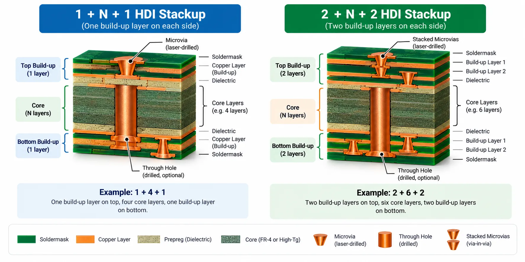
An HDI stackup is usually written in the form i+N+i, where N is the conventionally drilled core and each i is a sequentially laminated build-up layer added to that side.
So 1+N+1 means one build-up layer on each face of the core. 2+N+2 means two, which requires a second lamination cycle. The pattern continues to 3+N+3 and beyond, and each step adds a full press cycle to the schedule and the price.
At the far end sits any-layer construction, often sold as ELIC or every-layer interconnect, where every layer pair is joined by microvias and there is no conventionally drilled core at all.
Treat this notation as fabrication shorthand rather than as a classification. It tells you how many build-up layers and lamination cycles you are buying. It does not, on its own, tell you which IPC type your board is, because that also depends on what the core contains.
Both pieces of vocabulary are useful. They just answer different questions.
HDI PCB vs Standard PCB
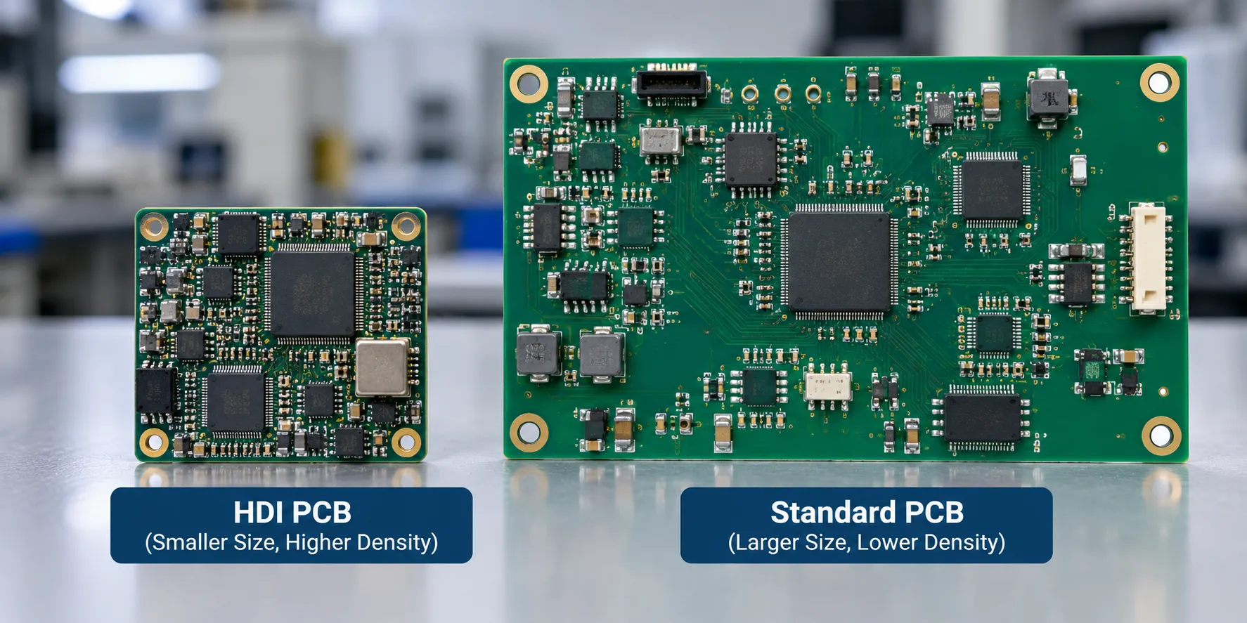
The difference between an HDI PCB and a standard PCB is how layers get connected. A standard board drills through the stack mechanically; a high-density board adds laser-drilled microvias between adjacent layers.
| HDI PCB | Standard PCB | |
|---|---|---|
| Via formation | Laser drilled microvias, plus mechanical | Mechanical drilling only |
| Via reach | Adjacent layers, locally | Through the whole stack |
| Lamination | Sequential, several press cycles | Single press |
| Line and space | Fine-line, well below standard | Standard fabrication limits |
| Layer count for a given design | Often fewer | Often more |
| Fabrication cost per panel | Higher | Lower |
| Fine-pitch BGA escape | Practical | Frequently impossible |
That fifth row is the one people miss. Because a microvia does not consume space on layers it never reaches, a high-density board can sometimes do in six layers what a conventional multilayer PCB needed ten to do.
When that happens, the cost comparison is not as one-sided as the per-panel price suggests. It is still usually more expensive, but not always by as much as expected.
The materials question changes too, since thin build-up dielectrics behave differently from standard PCB laminate, and the copper foil used on build-up layers is typically thinner than on a conventional press.
Choosing the right PCB laminate is its own decision, and I have set out the substrate options in my guide to PCB materials.
How Are HDI PCBs Manufactured?
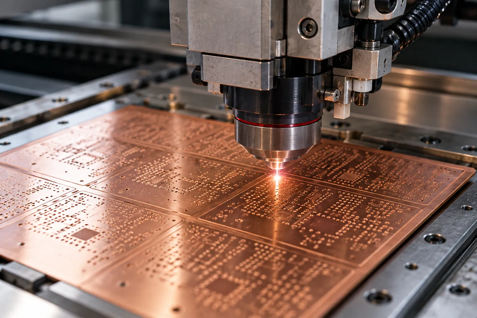
The HDI PCB manufacturing process builds the board outward from a core in stages, rather than pressing every layer together at once.
- Build and drill the core. The inner layers are imaged and, where the design calls for buried vias, mechanically drilled and plated before anything is added on top.
- Laminate the next layer. A thin dielectric and a sheet of copper foil are pressed onto each face of the core, the copper foil here being thinner than a conventional build would use.
- Laser drill the microvias. The laser ablates through the copper and dielectric down to the pad beneath, without touching layers below it.
- Metallize and fill. The microvias are plated, then filled, commonly with electroplated copper so the surface can be capped and used as a pad.
- Image and etch. The new outer layer is patterned to its fine-line geometry.
- Repeat for each build-up layer. Every additional pair of build-up layers means going round again.
- Finish the board. Surface finish, solder mask, electrical test and profiling follow as usual.
Sequential build-up is the name for that loop, and it explains the cost structure completely. You are not paying for a more difficult board so much as for running a board through lamination several times.
It also explains the yield risk. Each cycle is another chance for registration to drift or for the panel to warp, and a fault found at cycle four wastes everything from cycles one through three.
What Limits HDI Fabrication?
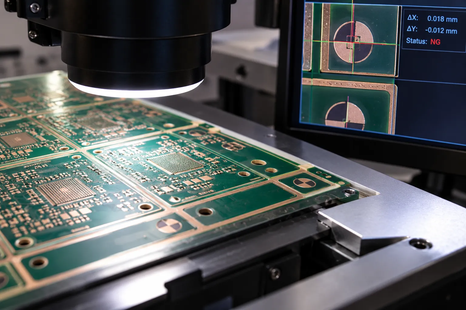
Four things set the practical limits, and every one of them is a conversation to have with your fabricator rather than a number to read off a datasheet.
- Laser aperture against copper thickness. The laser has to get through the copper before it reaches the dielectric. Thicker copper needs more energy, which widens the hole and eats into the aspect ratio budget you were relying on.
- Registration across lamination cycles. Each press shifts the panel slightly. By the third or fourth build-up layer, the accumulated drift is what decides whether a microvia lands on its target pad or half off it.
- Panel warpage. Thin dielectrics and repeated heat cycles leave a panel that does not sit flat, and a panel that does not sit flat does not image or drill accurately.
- Copper fill quality. Voiding and incomplete filling inside a microvia measurably shorten its fatigue life, which is the same failure mechanism behind the stacked-via problem above.
None of these are exotic. They are the ordinary consequences of doing lamination four times instead of once.
The practical upshot is that capability varies more between fabricators for high-density work than for conventional boards. Two shops quoting the same 2+N+2 stackup may be offering genuinely different things, and the cheaper quote is sometimes cheaper because it is running closer to its own limits.
Ask for the capability sheet, and ask what their yield looks like at the geometry you are specifying rather than at their headline minimum.
When Is HDI Worth the Cost?
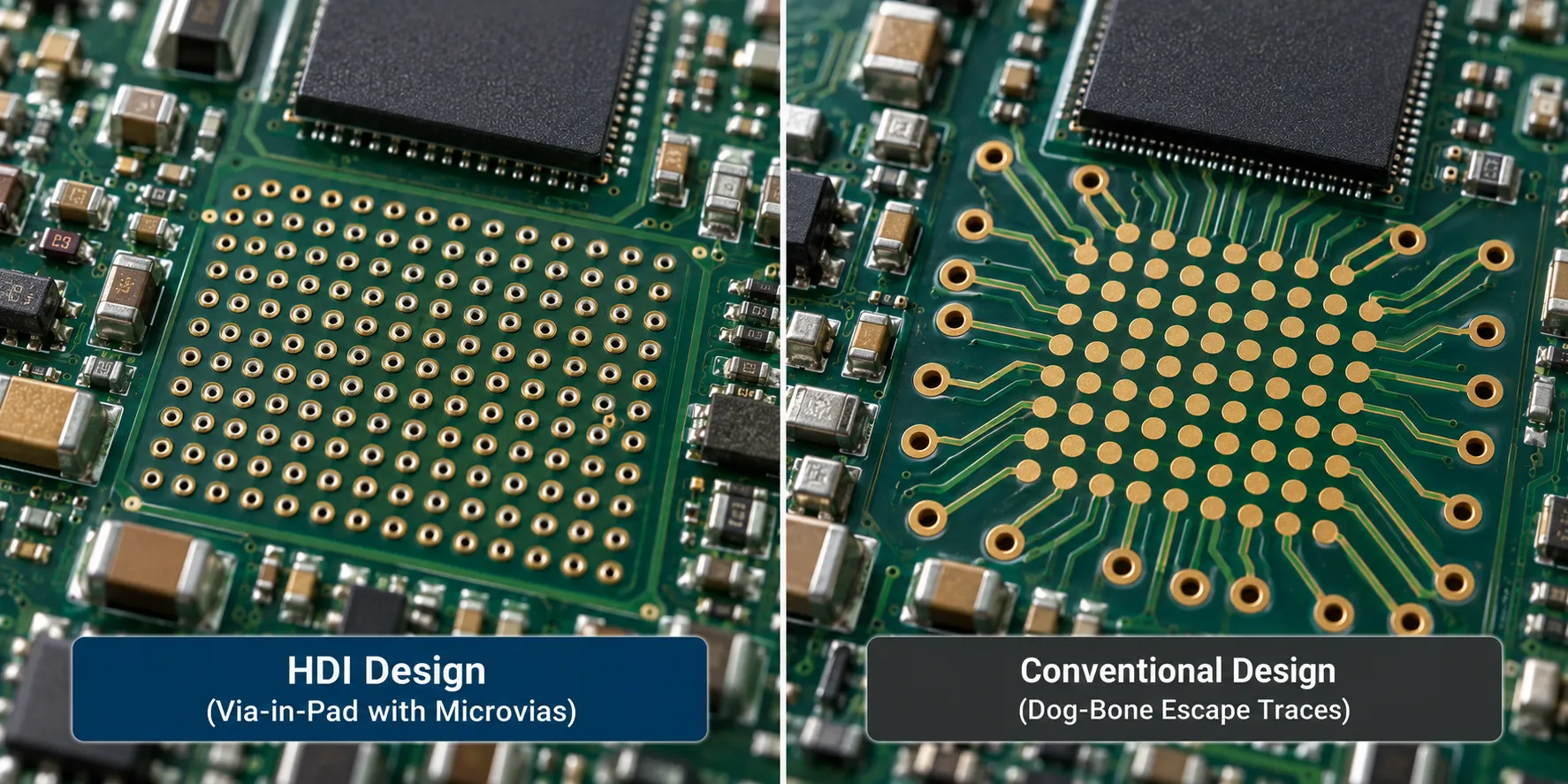
High-density interconnect is worth the cost when the design cannot route without it, or when it removes enough layers to pay for itself. Those are the two honest reasons.
Go with it when:
- A fine-pitch part leaves no room for an escape trace between pads.
- Board area or thickness is genuinely constrained by the product, not by preference.
- High-speed signals need the shorter paths and tighter impedance control that thin dielectrics allow.
- Removing layers offsets a meaningful part of the added process cost.
Do not go with it when the only driver is that the board looks crowded in the layout tool. Crowding is often a placement problem, and moving parts is free while adding lamination cycles is not.
My honest caveat: if your design sits near the boundary, get a fabricator to quote both constructions before committing. I have seen that comparison go both ways, and the general rule of thumb is not reliable enough to skip the quote.
The generic rules that still apply underneath all of this live in IPC-2221, the Generic Standard on Printed Board Design. The current revision is IPC-2221C, published in 2023 to supersede the 2012 B revision.
IPC-2226A is the HDI-specific section that sits on top of IPC-2221 rather than replacing it, so both apply to your board at once.
Getting this right is a layout decision, so it belongs in a design for manufacturability review, and the broader groundwork is in my guide to PCB layout design.
Frequently Asked Questions
How small can a microvia be?
Production microvias commonly land somewhere between 50 and 150 microns in diameter, with the depth constrained by the aspect ratio limit rather than by the laser. Ask your fabricator for their actual capability rather than designing to a general figure, because the economical size and the achievable size are rarely the same number.
Does HDI always mean more layers?
Often the opposite. Because microvias only occupy the layers they connect, routing that needed ten conventional layers can sometimes be done in six. The saving is real but not guaranteed, and it depends on how much of your congestion came from through-hole vias blocking inner layers.
Can I put a via in a component pad?
Yes, and on fine-pitch parts you usually must. The via has to be filled and capped first, because an open hole in a pad wicks solder away during reflow and starves the joint. Filled and plated-over via-in-pad is a standard HDI capability and a normal line item on a quote.
What is the difference between a blind via and a microvia?
Blind describes where it goes; microvia describes how big it is. A blind via connects an outer layer to an inner one without passing through the board, and it might be mechanically drilled. A microvia is defined by its aspect ratio and depth, and is laser formed. Most microvias are blind, but not all blind vias are microvias.
Are stacked microvias reliable?
They work, but reliability falls off as stacks get deeper, and published research shows a large gap between two-level and four-level stacks under thermal cycling. Stagger where the layout allows it, keep stacks shallow where it does not, and raise deep stacks explicitly at design review rather than letting them pass unnoticed.
Why does HDI cost more per panel?
Sequential build-up. Each pair of build-up layers means another lamination cycle, another laser drilling step, another plating and imaging pass. You are paying for repeated trips through the process, plus the yield risk that a late-stage defect scraps all the earlier work.