
THE 30-SECOND VERSION
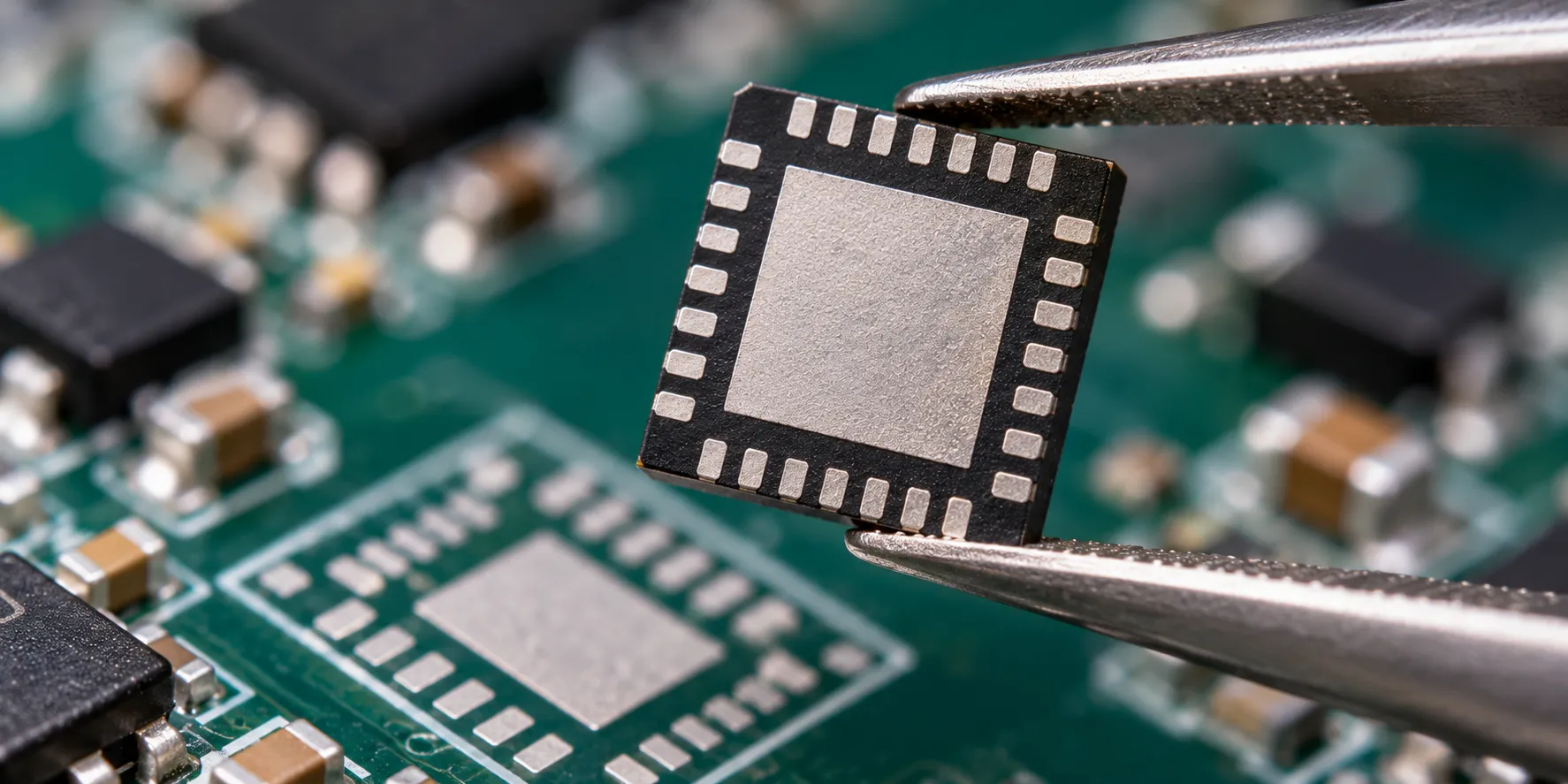
A QFN package is a leadless integrated circuit package with connection pads around the underside edge and a large exposed thermal pad in the middle.
It is smaller, cooler-running, and better at high frequency than a leaded equivalent. It is also unforgiving: the thermal pad drives most of the assembly problems, and the standard advice about voids that people carry over from BGA work does not apply here.
Most articles about the QFN package describe what it is and stop. That leaves out the part that actually costs people money, which is that the big metal pad in the middle behaves nothing like the small pads around the edge.
Here is my flat opinion. This is the package most often specified by someone who has never assembled one. It looks simple on a datasheet, it is cheap, it saves board space, and none of that tells you that paste volume on the centre pad will decide whether your part sits flat or floats.
So the thermal pad gets its own section below, with a finding that surprised me when I first read it.
What Is a QFN Package?
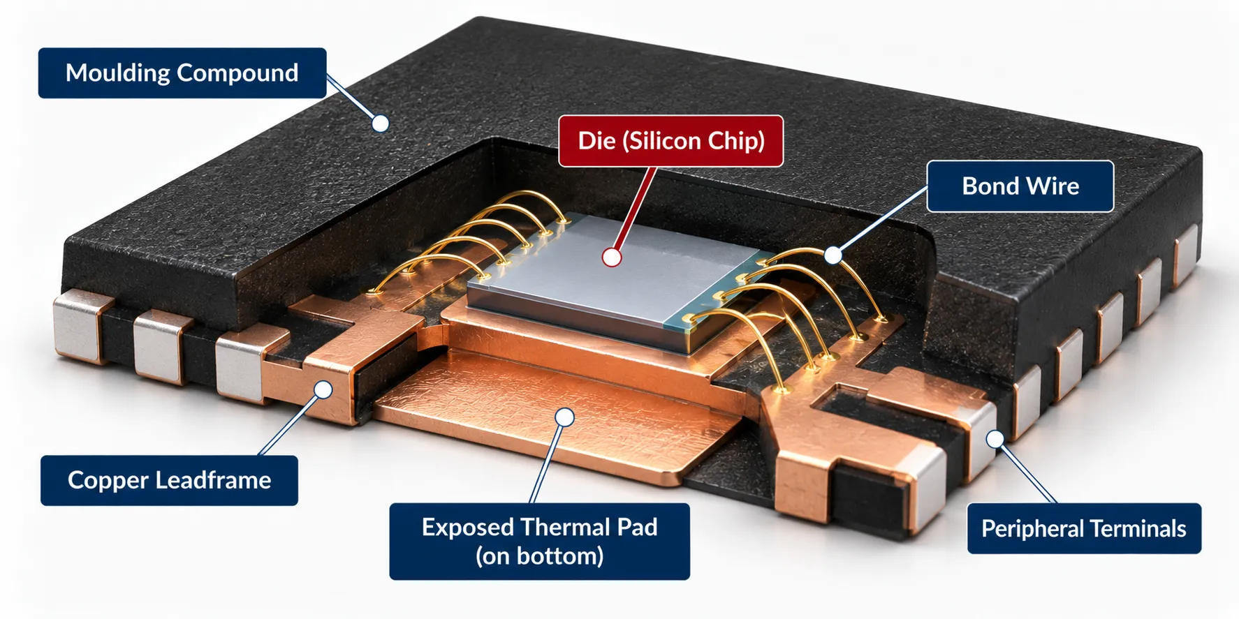
A QFN package, short for quad flat no-lead package, is a leadless semiconductor package whose connections are flat pads on the bottom face rather than leads extending from the sides. It is a surface-mount device, so it is soldered onto pads on the printed circuit board surface like any other.
Picture the difference between a spider and a limpet. A leaded part stands on legs that reach out beyond its body; this one sits flat against the board with its contacts underneath, touching nothing outside its own outline.
That is why it is called leadless. There is no metal sticking out to bend, to take up board space, or to add inductance between the die and the copper.
The quad flat no-lead format spread as integrated circuit packaging shrank and designers ran out of edge to put leads on.
What Is Inside One?
Inside the moulding is a copper leadframe, a silicon die, and the wires or bumps connecting them. The die is the integrated circuit itself, and everything around it exists to connect it and cool it.
The copper leadframe does double duty. It forms the perimeter contacts, and its central portion is left exposed at the bottom as the thermal pad, a direct metal path from the die down into the board.
That exposed pad is why this semiconductor package runs cooler than a leaded part of the same size. It is also, as you will see, why it is harder to assemble.
QFN and Bottom-Terminated Components
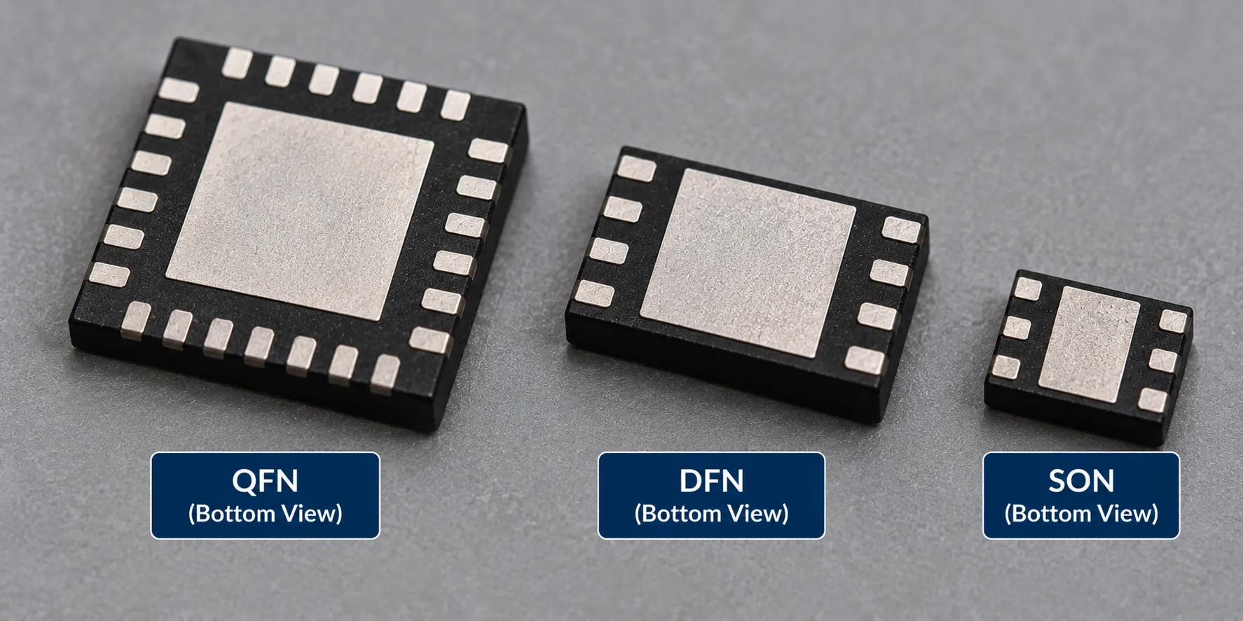
The quad flat no-lead belongs to a family the industry calls bottom-terminated components (BTCs), meaning any package whose terminations sit flat on its underside with no leads to inspect or probe. You will also see the singular form, bottom-termination package, used for an individual part of this kind.
The family shares a set of problems rather than a shape. Wikipedia lists the close relatives: DFN with pads on two sides instead of four, SON, and the micro leadframe packages sold as MLF or MLP, with dual-row variants reaching into the hundreds of connections.
Knowing the category name matters because that is how the standards index it. The document written for these parts is IPC-7093A, Design and Assembly Process Implementation for Bottom Termination Components.
IPC released revision A on 15 February 2021, describing it as a complete overhaul of the original 2011 standard.
What the overhaul added is exactly what this article is about: guidance on thermal pad design, thermal via usage, stencil design, and troubleshooting assembly anomalies. If a supplier quotes you IPC-7093 without the letter, ask which revision they mean.
What Are the Types of QFN Packages?
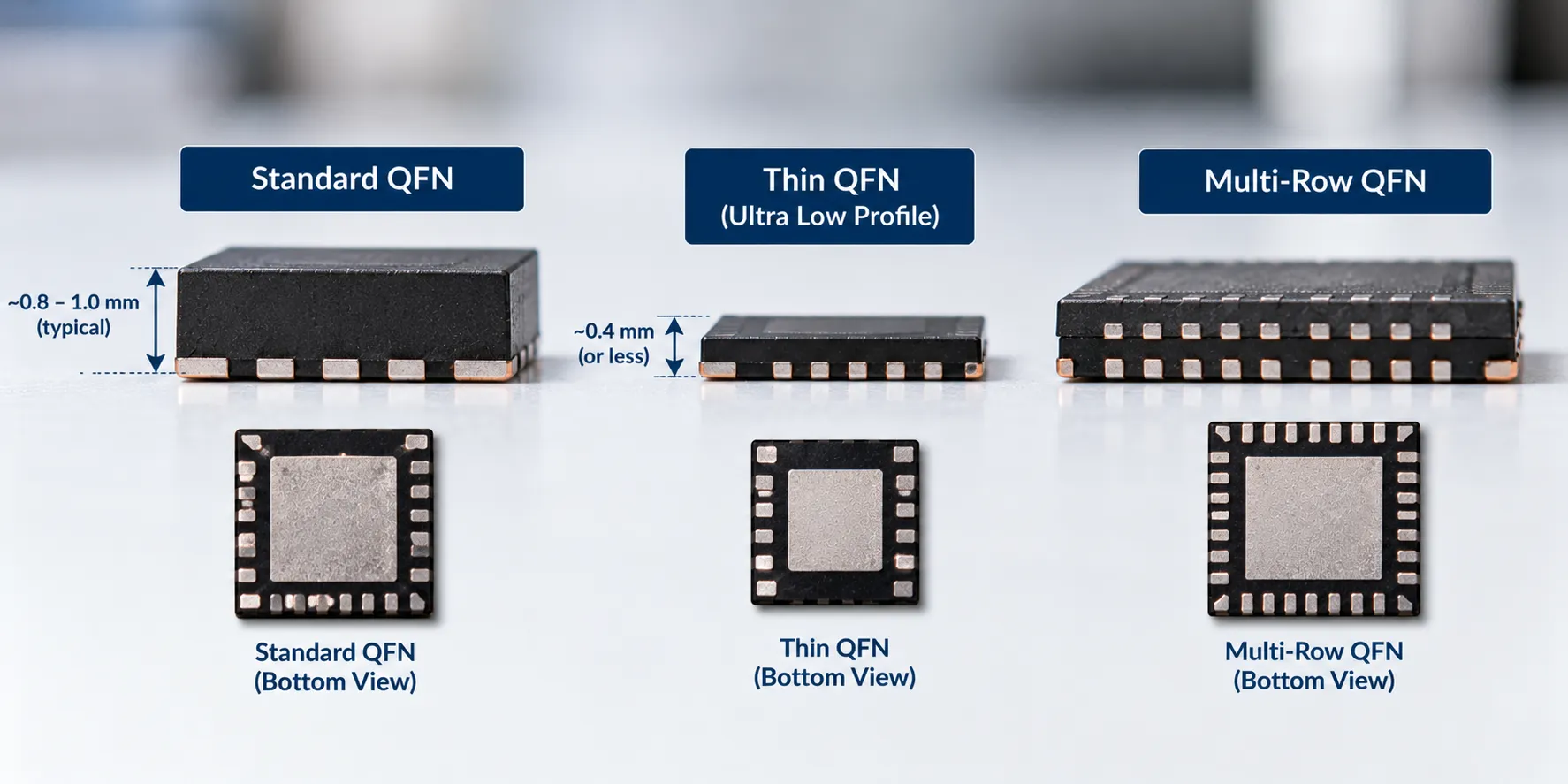
QFN package types differ in three ways: how thick the body is, how many rows of pads it carries, and how the parts were separated during manufacture.
| Variant | What distinguishes it | Why it matters to you |
|---|---|---|
| Standard QFN | Baseline body height | The common case |
| TQFN, VQFN, UQFN | Thin, very thin, ultra thin bodies | Less thermal mass, easier to warp |
| DFN | Pads on two sides only | Simpler, fewer connections |
| Multi-row QFN | Two or more rows of perimeter pads | Higher pin count, much harder to inspect |
| Punched | Singulated by punching, one part per mould | Slightly tapered sidewalls, common at low volume |
| Sawn | Singulated by sawing a moulded array | Straight sidewalls, preferred at high volume |
The punched and sawn distinction sounds like a factory detail you can ignore. It is not, because it changes whether the pad sidewall is exposed metal that solder can climb.
A sawn part often shows a wettable flank, a plated side surface that lets a visible fillet form. If you want a joint an optical camera can actually see, that is the feature to ask your supplier about.
QFN vs QFP: What Actually Changes?
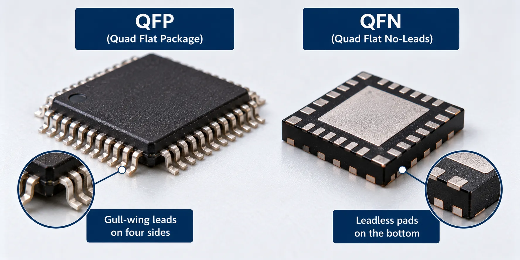
The difference between a QFN vs QFP package is that a QFP stands on gull-wing leads around its edge, while a QFN sits flat on pads underneath it.
Everything else follows from that one structural fact.
| QFN | QFP | |
|---|---|---|
| Connections | Flat pads under the body | Gull-wing leads at the sides |
| Board area | Smaller, no lead overhang | Larger for the same pin count |
| Inductance | Lower, better at high frequency | Higher |
| Heat path | Down through the thermal pad | Out through thin leads |
| Inspection | X-ray, joints are hidden | Visual, every joint is exposed |
| Hand rework | Hard, needs hot air | Straightforward with an iron |
| Compliance to board | None, the part is rigid | Leads flex and absorb stress |
That last row is the one people underestimate. A gull-wing lead is a small spring, so it absorbs the mismatch between a package and a board expanding at different rates.
A leadless part has no such give. The solder joint takes that stress directly, which is why thermal cycling behaviour deserves attention on parts that will run hot and cold repeatedly.
Choose the leadless part when board space, height, or high-frequency behaviour actually constrain the design. Choose the leaded one when you want easy inspection, easy repair, and a quieter life.
Why the Thermal Pad Causes Most QFN Problems
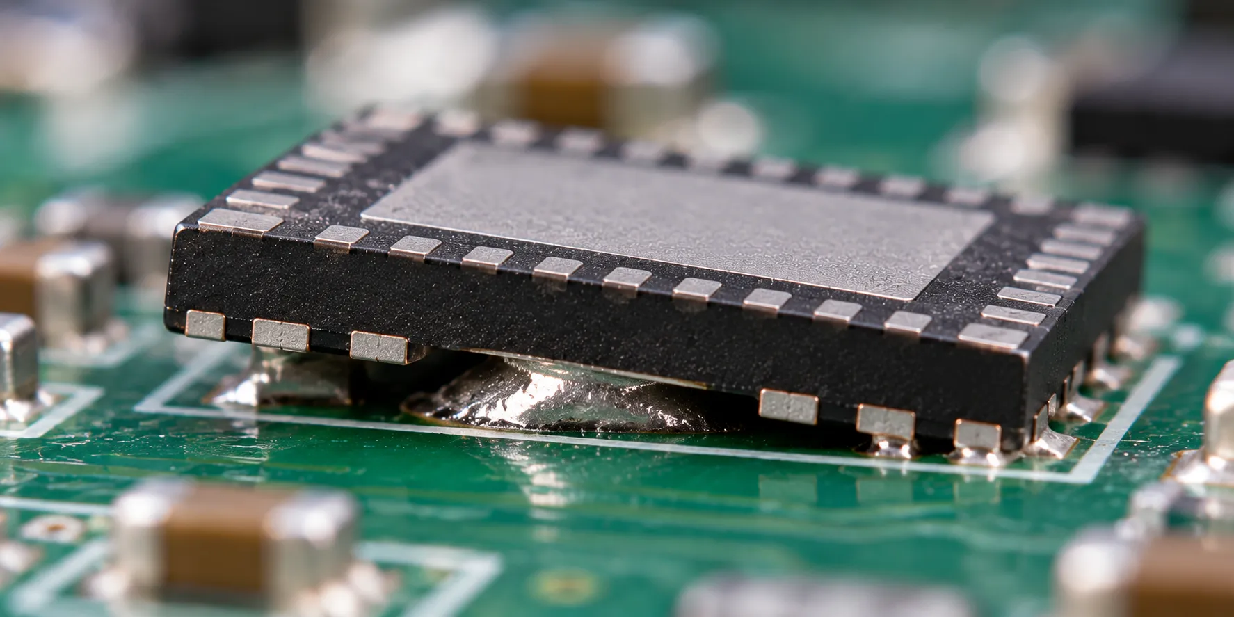
The exposed thermal pad causes most QFN assembly problems because it is far larger than any perimeter pad, and a large pad printed with a matching volume of paste lifts the part off the board.
Here is the mechanism. Inside the reflow oven, molten solder under the centre pad has surface tension pulling it into a dome. If there is too much of it, the package rides up on that dome like a car on a jack.
The perimeter joints then either stretch thin or open completely. Each one becomes a solder joint you cannot see and cannot probe, and the board may even work until it is dropped or heated.
The fix is not more heat or a different profile. It is less paste on the centre pad, applied as several separate deposits rather than one large one.
How Much Voiding Is Actually Acceptable?
More than you probably think, and this is where instinct carried over from BGA work leads people wrong.
A BGA ball is a structural joint, so a void in it is lost strength. The centre pad here is mostly a heat path, and it has area to spare.
A study by Derrick Herron, Yan Liu and Ning-Cheng Lee of Indium Corporation tested this directly, presented at the Pan Pacific Conference in January 2011.
They found thermal performance held up with void content reaching 50 percent, even 60 percent, of the pad area.
Treat that as context, not as a licence. Your own acceptance criteria come from the standard your contract names, and perimeter joints are judged far more strictly than the centre pad.
The same study found the most effective single fix for voiding was plugging the thermal vias, and recommended dividing the thermal pad rather than using one solid area when the via count is high.
How Do You Design the Footprint and Stencil?
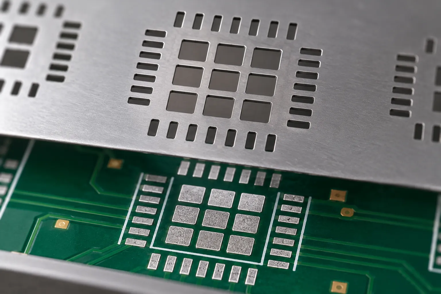
Design the stencil before you worry about the reflow profile, because that is where the outcome is decided.
- Split the thermal pad aperture. Use a grid of smaller openings, the windowpane pattern, rather than one large one. The Indium work describes typical practice as multiple openings covering roughly 50 to 80 percent of the pad, separated by gaps of a few tenths of a millimetre.
- Give outgassing somewhere to go. Those gaps between deposits are escape routes for flux volatiles. A solid deposit traps them as voids.
- Plug or cap thermal vias. An open via under the pad wicks solder down into the barrel, starving the joint and leaving a cavity behind.
- Follow the manufacturer’s land pattern. Semiconductor makers publish application notes for their own packages, and those override generic advice.
- Keep the perimeter apertures modest. Overprinting the small pads bridges them, and there is no lead standing clear of the board to absorb the excess.
Two of those bullets, via plugging and windowpane apertures, do most of the work. If you only change two things on a troublesome design, change those, and change them before the board ever reaches a reflow oven.
This is squarely a layout decision rather than a production one, which is why it belongs in a design for manufacturability review, and why PCB layout design choices here are expensive to reverse later.
How Are QFN Joints Inspected and Reworked?
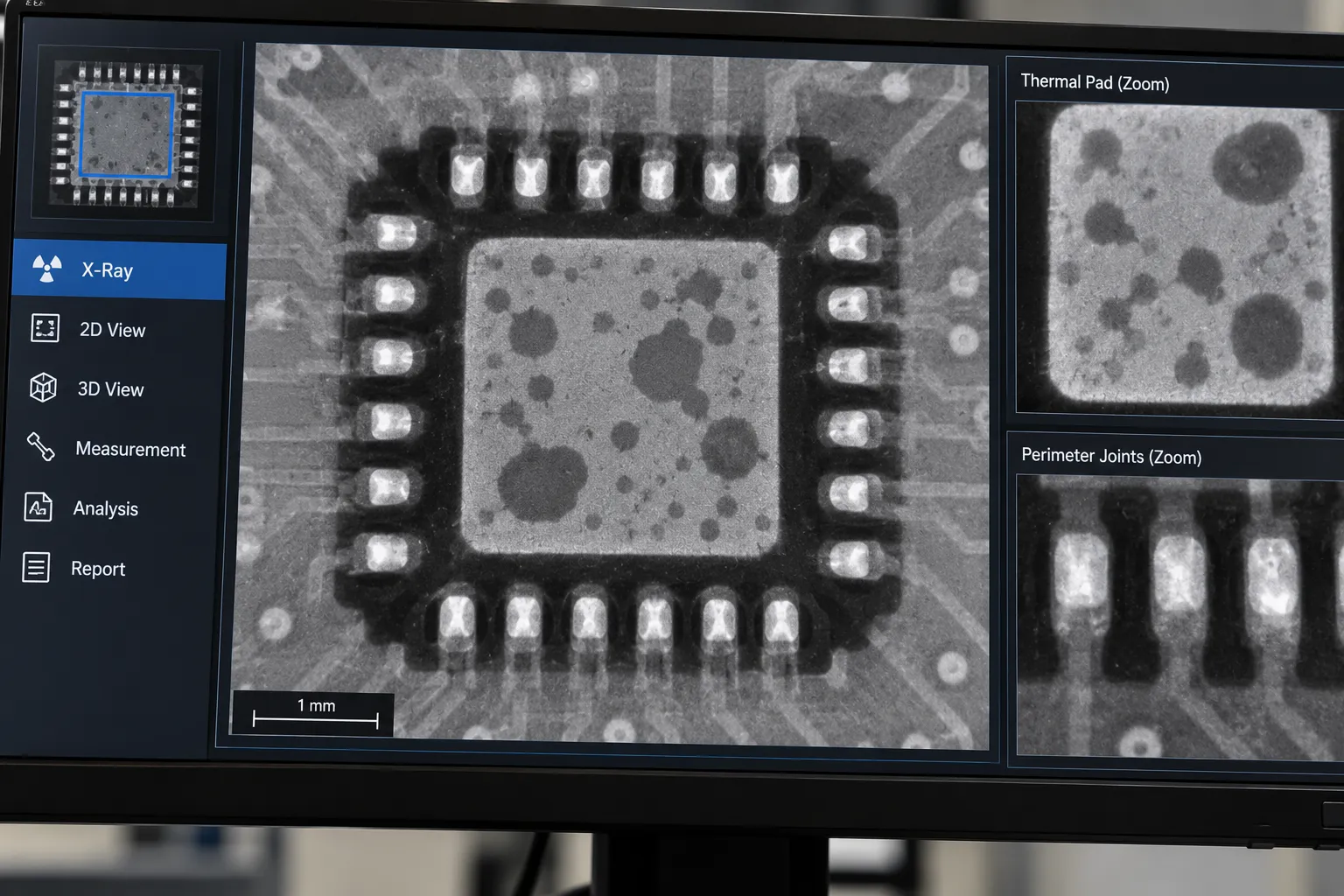
These joints are checked by X-ray inspection because the perimeter pads and the centre pad all sit under the package body.
An X-ray shows the perimeter joints as small shapes around the outline, and the thermal pad as a large area with any voids visible as lighter patches inside it. What it does not show well is joint height, so a package floating on its centre pad can pass a casual look.
Optical inspection still earns its place on a surface-mount device with wettable flanks, where a camera can see a real fillet climbing the plated side of the pad. Without that feature, there is nothing to photograph.
X-ray sits inside a wider set of checks, and I have compared them in my guide to PCB testing methods.
Rework follows the same pattern as any hidden-joint package: localised heat from a rework station, a vacuum lift, pads wiped clean, fresh paste, and a second reflow. The difference is the centre pad, which holds heat and resists release longer than the small perimeter joints.
Much of this will feel familiar if you work with the other hidden-joint package, and the parallels and differences are covered in my guide to BGA assembly.
The profile matters as much on a second pass as on the first, and I have set out how to build one in my guide to reflow soldering.
Frequently Asked Questions
Can you hand-solder a QFN package?
The perimeter pads yes, with flux, a fine tip, and patience working from the outside. The thermal pad is the problem, because you cannot reach it. Some designs add a via under the centre pad so solder can be fed from the back, but that is a design decision, not a rescue for a board already made.
Why is my QFN floating or tilting after reflow?
Too much paste on the thermal pad. Molten solder domes under the centre and lifts the package, opening the perimeter joints. Reduce thermal pad coverage using a windowpane stencil pattern rather than one large aperture, and check that the perimeter apertures are not overprinted at the same time.
Does every QFN need X-ray inspection?
Every new design and every process change, yes. Once a design runs with stable results, sampling is reasonable. Parts with wettable flanks are the exception worth asking about, since they give an optical camera something real to judge.
What is the difference between QFN and DFN?
Pad placement. A quad flat no-lead has pads on all four sides of the package, a DFN on two opposite sides only. Both are bottom-terminated components with the same thermal pad behaviour, so the assembly guidance in this article applies to both.
Do QFN packages need thermal vias?
Usually, if the part dissipates real power. The exposed pad is a heat path into the board, and without vias carrying that heat into an inner plane of the printed circuit board it stops at the surface layer. Plug or cap them, though, because open vias under the pad pull solder away from the joint.
Are QFN packages reliable under thermal cycling?
They are used successfully in demanding products, but the joints carry stress that a leaded package would absorb in its leads. For assemblies that swing through wide temperature ranges repeatedly, this is a question to raise at design review rather than after qualification testing.